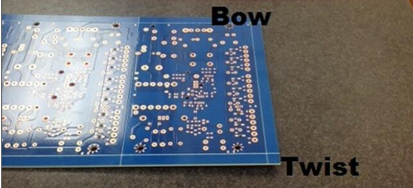
Why does the PCB board warp? Why does it cause so much harm after deformation?
The dangers of PCB board deformation
In automated surface mounting lines, if the circuit board is not flat, it will cause inaccurate positioning, components cannot be inserted or mounted into the board’s holes and surface mounting pads, and the automatic insertion machine may even be damaged.
The circuit board with the components on it is bent after soldering, and it is difficult to cut the component pins neatly. The board cannot be installed into the chassis or the socket inside the machine, so it is also very troublesome for the assembly factory to encounter a warped board.
The current surface mount technology is developing in the direction of high precision, high speed and intelligence, which puts forward higher flatness requirements for PCB boards, which are the homes of various components.
In the IPC standard, it is specifically stated that the allowable deformation of PCB boards with surface mount devices is 0.75%, and the allowable deformation of PCB boards without surface mount devices is 1.5%.
In fact, in order to meet the needs of high-precision and high-speed placement, some electronic assembly manufacturers have stricter requirements for deformation. If required, the allowed deformation is 0.5%, and some even require 0.3%.
PCB boards are composed of copper foil, resin, glass cloth and other materials. The physical and chemical properties of each material are different. After being pressed together, thermal stress residues will inevitably occur, leading to deformation.
At the same time, during the processing of PCB, various processes such as high temperature, mechanical cutting, and wet treatment will also have an important impact on the deformation of the board. In short, the causes of PCB board deformation are complex and diverse. How to reduce or eliminate the deformation due to material characteristics? Deformation caused by differences or processing has become one of the complex problems faced by PCB manufacturers.
Analysis of causes of PCB board deformation
The deformation of PCB board needs to be studied from several aspects such as material, structure, pattern distribution, processing process, etc. This article will analyze and elaborate on the various causes of possible deformation and improvement methods.
The uneven copper surface area on the circuit board will worsen the board bending and warping.
Generally, circuit boards are designed with a large area of copper foil for grounding purposes. Sometimes the Vcc layer is also designed with a large area of copper foil. When these large area copper foils cannot be evenly distributed on the same circuit board When it is installed, it will cause the problem of uneven heat absorption and heat dissipation speed.
Of course, the circuit board will also expand due to thermal expansion and contraction. If the expansion and contraction cannot occur at the same time, it will cause different stresses and deformation. At this time, if the temperature of the board has reached the upper limit of the Tg value, the board will begin to soften, causing deformation.
The connection points (vias, vias) of each layer on the circuit board will limit the expansion and contraction of the board.
Most of today’s circuit boards are multi-layer boards, and there are connection points (vias) like rivets between layers. The connection points are divided into through holes, blind holes and buried holes. Where there are connection points, the board will be restricted. The effect of expansion and contraction will also indirectly cause the board to bend and warp.
Reasons for PCB board deformation:
(1) The weight of the circuit board itself will cause the board to dent and deform.
Generally, reflow furnaces use chains to drive the circuit board forward in the reflow furnace, that is, using both sides of the board as fulcrums to support the entire board.
If there are overweight parts on the board, or the size of the board is too large, there will be a dent in the middle due to its own weight, causing the board to bend.
(2) The depth of the V-Cut and the connecting strip will affect the deformation of the panel.
Basically, V-Cut is the culprit that destroys the structure of the board. Because V-Cut cuts grooves into the original large sheet, the V-Cut is prone to deformation.
The influence of laminating materials, structures, and graphics on plate deformation:
The PCB board is composed of a core board, a prepreg, and an outer layer of copper foil. The core board and copper foil are thermally deformed during lamination. The amount of deformation depends on the coefficient of thermal expansion (CTE) of the two materials.
The thermal expansion coefficient (CTE) of copper foil is about 17X10-6; while the Z-direction CTE of ordinary FR-4 substrate at the Tg point is (50~70)X10-6; above the TG point it is (250~350)X10-6 , X-direction CTE is generally similar to copper foil due to the presence of glass cloth.
Deformation caused during PCB board processing
The causes of PCB board deformation during processing are very complex and can be divided into two types of stress: thermal stress and mechanical stress.
Thermal stress is mainly generated during the lamination process, and mechanical stress is mainly generated during the stacking, handling, and baking processes of panels. The following is a brief discussion in process order.
1. Incoming copper clad laminate materials:
Copper-clad laminates are all double-sided with symmetrical structure and no graphics. The CTE of copper foil and glass cloth are almost the same, so there is almost no deformation caused by different CTE during the lamination process.
However, the size of the copper-clad laminate press is large, and there are temperature differences in different areas of the hot plate, which will lead to slight differences in the resin curing speed and degree in different areas during the lamination process. At the same time, the dynamic viscosity at different heating rates is also significantly different, so there will also be Local stresses due to differences in the curing process.
Generally, this stress will maintain balance after pressing, but will gradually release and cause deformation during subsequent processing.
2. Pressing:
The PCB lamination process is the main process that generates thermal stress. Similar to the lamination of copper-clad laminates, it will also produce local stress caused by differences in the curing process. The thermal stress of PCB boards is due to thicker thickness, diverse pattern distribution, and more prepregs. The stress will also be more difficult to eliminate than that of copper clad laminate.
The stress existing in the PCB board is released during subsequent drilling, shaping or grilling processes, causing the board to deform.
3. Baking process of solder mask, characters, etc.:
Since the solder mask ink cannot be stacked on top of each other when curing, the PCB boards will be placed vertically in a rack for curing. The solder mask temperature is about 150°C, which is just above the Tg point of medium and low Tg materials. The resin above the Tg point is in a highly elastic state, and the board Parts are easily deformed under their own weight or strong wind from the oven.
4. Hot air solder leveling:
When leveling hot air solder for ordinary boards, the tin furnace temperature is 225℃~265℃ and the time is 3S-6S. The hot air temperature is 280℃~300℃.
The solder leveling plate enters the tin furnace at room temperature, and is post-processed and washed at room temperature within two minutes after coming out of the furnace. The entire hot air solder leveling process is a sudden heating and cooling process.
Due to different circuit board materials and uneven structures, thermal stress will inevitably occur during the cooling and heating process, resulting in microscopic strain and overall deformation and warping.
5. Storage:
PCB boards are generally stored vertically in racks during the semi-finished product stage. Improper adjustment of the rack’s tightness or stacking of boards during storage will cause mechanical deformation of the boards. Especially for thin plates below 2.0mm, the impact is more serious.
In addition to the above factors, there are many factors that affect PCB board deformation.
Prevention of PCB board warpage and deformation
Circuit board warpage has a great impact on the production of printed circuit boards. Warpage is also one of the important problems in the circuit board production process. The board with components on it will bend after welding, making it difficult for the component legs to be neat.
The board cannot be installed into the chassis or the socket inside the machine. Therefore, the warping of the circuit board will affect the normal operation of the entire subsequent process.
At this stage, printed circuit boards have entered the era of surface mounting and chip mounting, and the process requirements for circuit board warpage are getting higher and higher. So we need to find the reason why the circuit board is warping.
1. Engineering design:
Things to note when designing printed circuit boards:
A. The arrangement of prepreg sheets between layers should be symmetrical. For example, for a six-layer board, the thickness between layers 1 to 2 and 5 to 6 should be consistent with the number of prepreg sheets, otherwise it will easily warp after lamination.
B. Multilayer core boards and prepregs should use products from the same supplier.
C. The line pattern areas on the outer layer A and B should be as close as possible. If side A is a large copper surface and side B only has a few lines, this kind of printed board will easily warp after etching. If the line areas on the two sides are too different, you can add some independent grids on the sparse side for balance.
2. Drying plate before unloading:
The purpose of drying the copper-clad laminate (150 degrees Celsius, 8 ± 2 hours) before unloading is to remove the moisture in the board, and at the same time completely solidify the resin in the board, further eliminating the remaining stress in the board, which is helpful in preventing the board from warping. helpful.
At present, many double-sided and multi-layer boards still adhere to the step of drying the boards before or after cutting. However, there are exceptions for some board factories. Currently, the drying time regulations of various PCB factories are inconsistent, ranging from 4 to 10 hours. It is recommended to decide based on the grade of the printed boards produced and the customer’s requirements for warpage.
Both methods are feasible, whether to cut the pieces into panels and then bake them or to bake them as a whole piece and cut them out. It is recommended to cut the materials and then bake them. The inner layer boards should also be baked.
3. Longitude and latitude direction of prepreg:
The warp and weft shrinkage rates of prepregs after lamination are different, and the warp and weft directions must be distinguished when blanking and laminating. Otherwise, it is easy to cause the finished board to warp after lamination, which is difficult to correct even if pressure is applied to bake the board.
Many reasons for the warping of multi-layer boards are caused by not distinguishing the longitude and weft directions of the prepreg sheets during lamination, and they are stacked randomly.
How to distinguish longitude and latitude? The rolling direction of the rolled prepreg is the warp direction, and the width direction is the weft direction; for copper foil boards, the long side is the weft direction, and the short side is the warp direction. If you are not sure, you can check with the manufacturer or supplier.
4. Stress relief after lamination:
After completing the hot and cold pressing, the multi-layer board is taken out, the burrs are cut or milled, and then placed flat in an oven at 150 degrees Celsius for 4 hours to gradually release the stress in the board and completely solidify the resin. This step cannot be omitted.
5. Thin sheets need to be straightened during electroplating:
When using 0.4~0.6mm ultra-thin multi-layer boards for surface electroplating and pattern electroplating, special clamp rollers should be made. After clamping the thin plate on the fly bar of the automatic electroplating line, use a round stick to clamp the entire fly bar. The rollers are strung together to straighten all the boards on the rollers so that the plated boards will not deform.
Without this measure, the sheet will bend after plating a copper layer of 20 to 30 microns, and it will be difficult to repair.
6. Cooling of the board after hot air leveling:
During hot air leveling, the printed board is subjected to the high temperature impact of the soldering bath (about 250 degrees Celsius). After being taken out, it should be placed on a flat marble or steel plate to cool naturally, and then sent to the post-processing machine for cleaning. This is very good for preventing the board from warping.
In order to enhance the brightness of the lead-tin surface, some factories put the board into cold water immediately after being leveled with hot air, and then take it out after a few seconds for post-processing. This kind of hot and cold impact may cause warping of some types of boards. Curved, layered or blistered.
In addition, an air flotation bed can be installed on the equipment for cooling.
7. Treatment of warped boards:
In a well-managed factory, 100% flatness inspection of printed boards will be carried out during final inspection. All unqualified boards will be picked out, placed in an oven, baked at 150 degrees Celsius under heavy pressure for 3 to 6 hours, and allowed to cool naturally under heavy pressure.
Then remove the pressure and take out the board, and then check the flatness. This can save part of the board. Some boards need to be baked and pressed two to three times before they can be flattened. If the above-mentioned anti-warping process measures are not implemented, baking and pressing some boards will be useless and they will have to be scrapped.

