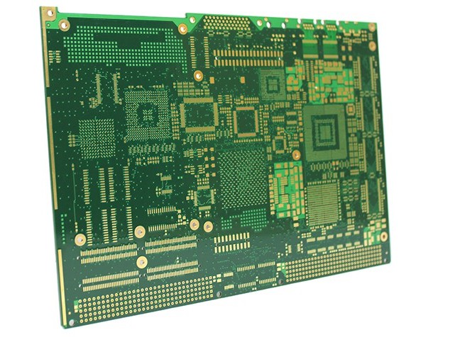
What is HDI PCB?
HDI PCB stands for High Density Interconnect Printed Circuit Board. Compared with traditional PCBs, HDI PCBs have higher circuit density, finer lines and spacing, and smaller via diameters. HDI PCBs use advanced manufacturing techniques such as laser drilling, stacked vias, and microvias to increase the packing density of components on the board, thereby reducing board size and improving signal integrity. HDI PCBs offer several advantages over traditional PCBs, including:
- Reduced board size: HDI PCBs allow more components to be packed into a smaller area, reducing overall board size.
- Faster signal transmission: HDI PCB has shorter signal paths due to the smaller distance between components, resulting in faster signal transmission between components.
- Improved reliability: HDI PCB has more interconnections between components, making it more reliable and less prone to failure.
- Higher thermal performance: HDI PCB conducts heat more efficiently, resulting in better thermal management of the board.
HDI PCBs are commonly used in high-performance electronic devices such as smartphones, tablets, and laptops, as well as in aerospace and military applications where size and weight reduction is critical.

