What impact does the stencil have on the processing quality of SMT patches?
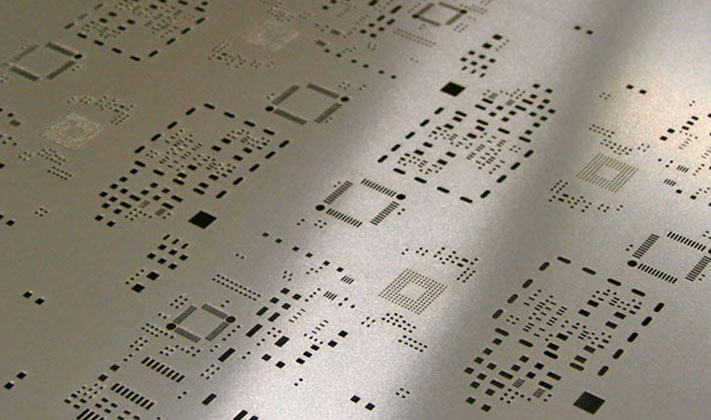
1. How to make stencil
At present, the main methods of making stencil are: chemical etching, laser cutting, and electroform.
Chemical etching has large errors and is not environmentally friendly; the data production accuracy is high and the influence of objective factors is small; the trapezoidal opening is conducive to demoulding; precision cutting can be done; the price is moderate; the hole wall is smooth, especially suitable for ultra-fine pitch steel mesh production method, and the price is high .
At present, most SMT chip processing factories use laser stencil, which is cost-effective and of good quality.
2. Stencil material
Generally, the steel mesh is made of stainless steel, which has high printing accuracy and long service life.
3. Stencil thickness
The thickness and size of the stencil directly determine the amount of tin on the pad, directly affecting whether problems such as virtual soldering and tin connection will occur.
Usually there are both components with a spacing of 1.27mm or more and components with a narrow spacing on a PCB. Components with a spacing of 1.27mm or more require a stainless steel plate 0.2mm thick, and components with a narrow spacing require a stainless steel plate 0.15-0.10mm thick. The thickness of the stainless steel plate can be determined based on the condition of most components on the PCB, and then the amount of solder paste leakage can be adjusted by expanding or reducing the size of the pad opening of individual components.
If there is a large difference in the amount of solder paste required for components on the same PCB, the template at the narrow-pitch components can be partially thinned, but the processing cost of the thinning process is higher. Therefore, a compromise method can be adopted. The thickness of the stainless steel plate can be an intermediate value. For example: some components on the same PCB require 0.20mm thickness, and other components require 0.15-0.12mm thickness. In this case, the thickness of the stainless steel plate can be 0.18 mm.
4. Stencil size
The opening size can be 1:1 for general components. For large Chip components and PLCC that require a large amount of solder paste, the opening area should be expanded by 10%. For devices such as QFP with pin spacing of 0.5mm and 0.65mm, the opening area should be reduced by 10%.
5. Stencil shape
Appropriate opening shape can improve the placement effect. For example: when the size of the chip component is smaller than 1005 and 0603, due to the small distance between the two pads, the solder paste on the pads at both ends can easily flow to the bottom of the component during placement. Adhesion, bridges and solder beads at the bottom of components can easily occur after reflow soldering. Therefore, when processing the template, the inside of the opening of a pair of rectangular pads (Figure 1) can be modified into a sharp angle or an arc shape (Figure, Chip component opening shape) to reduce the amount of solder paste at the bottom of the component, which can improve the component placement The solder paste on the bottom is sticking.
6. Stencil performance requirements
The frame is not deformable. The tension should be average and high, preferably 30 N/㎜? or above. The metal should be flat. The metal plate thickness error is less than ±10%. The opening should be aligned with the PCB (high accuracy). The opening section of the steel plate should be vertical, and the protruding part in the middle should not be greater than 15% of the thickness of the metal plate.
The dimensional accuracy of the opening of the steel plate for SMT patch processing must be within the tolerance ±0.01㎜ and shall not exceed 0.02㎜. The thickness and opening size of the stencil directly affect the amount of solder paste printed. During production, parameters such as the thickness and opening size of the stencil need to be confirmed to ensure the quality of solder paste printing.

