What are the PCB board materials?
Introduction to PCB circuit board materials:
The classification from bottom to top is as follows:
94HB/94VO/22F/CEM-1/CEM-3/FR-4
The details are as follows:
94HB: Ordinary cardboard, not fireproof (the lowest grade material, die-punched, cannot be used as a power board)
94V0: Flame retardant cardboard (die punching)
22F: Single-sided semi-fiberglass board (die punching)
CEM-1: Single-sided fiberglass board (must be computer drilled, not punched)
CEM-3: Double-sided semi-glass fiber board (except for double-sided cardboard, it is the lowest-end material for double-sided panels. Simple double-sided panels can use this material, which is 5~10 yuan/square meter cheaper than FR-4)
FR-4: Double-sided fiberglass board
Best answer
1.c The classification of flame retardant properties can be divided into four types: 94V-0/V-1/V-2 and 94-HB
2. Pre-cured sheet: 1080=0.0712mm, 2116=0.1143mm, 7628=0.1778mm
3. FR4 CEM-3 both represent boards, fr4 is fiberglass board, and cem3 is composite substrate
4. Halogen-free refers to substrates that do not contain halogens (fluorine, bromine, iodine and other elements), because bromine will produce toxic gases when burned, which is environmentally friendly.
6. Tg is the glass transition temperature, that is, the melting point.
Circuit boards must be flame-resistant and cannot burn at a certain temperature, only softening. The temperature point at this time is called the glass transition temperature (Tg point). This value is related to the dimensional stability of the PCB board.
What is a high Tg PCB circuit board and the advantages of using high Tg PCB
When the temperature of a high-Tg printed board rises to a certain area, the substrate will change from “glass state” to “rubber state”. The temperature at this time is called the glass transition temperature (Tg) of the board. In other words, Tg is the maximum temperature (°C) at which the substrate remains rigid. That is to say, ordinary PCB substrate materials not only soften, deform, melt, etc. under high temperatures, but also show a sharp decline in mechanical and electrical properties (I think you don’t want to see this happen to your products).
Generally, the Tg of the plate is above 130 degrees, the high Tg is generally above 170 degrees, and the medium Tg is about above 150 degrees.
Usually PCB printed boards with Tg≥170℃ are called high Tg printed boards.
As the Tg of the substrate increases, the heat resistance, moisture resistance, chemical resistance, stability resistance and other characteristics of the printed board will be increased and improved. The higher the TG value, the better the temperature resistance of the plate. Especially in the lead-free process, there are many high Tg applications.
High Tg refers to high heat resistance. With the rapid development of the electronics industry, especially electronic products represented by computers, which are developing towards high functionality and high multi-layering, higher heat resistance of PCB substrate materials is required as an important guarantee. The emergence and development of high-density mounting technologies represented by SMT and CMT have made PCBs increasingly inseparable from the support of high heat resistance of the substrate in terms of small apertures, fine wiring, and thinness.
Therefore, the difference between general FR-4 and high Tg FR-4 is: in the hot state, especially when heated after absorbing moisture, the material’s mechanical strength, dimensional stability, adhesion, water absorption, and thermal decomposition properties There are differences in various conditions such as thermal expansion and thermal expansion. High Tg products are obviously better than ordinary PCB substrate materials.
In recent years, the number of customers requesting the production of high-Tg printed boards has increased year by year.
PCB board knowledge and standards (2007/05/06 17:15)
At present, the following types of copper-clad laminates are widely used in our country. Their characteristics are shown in the table below: Types of copper-clad laminates, knowledge of copper-clad laminates
There are many ways to classify copper clad laminates. Generally, according to the different reinforcing materials of the board, it can be divided into: paper base, glass fiber cloth base,
There are five categories: composite base (CEM series), laminated multi-layer board base and special material base (ceramic, metal core base, etc.). If the panel is used
The resin adhesives are classified differently, the common paper-based CCI. There are: phenolic resin (XPc, XxxPC, FR-1, FR
-2 etc.), epoxy resin (FE-3), polyester resin and other types. Common fiberglass cloth-based CCLs include epoxy resin (FR-4, FR-5), which is currently the most widely used fiberglass cloth-based type. There are also other special resins (using glass fiber cloth, polyamide fiber, non-woven fabric, etc. as additional materials): bismaleimide-modified triazine resin (BT), polyimide resin (PI) , diphenylene ether resin (PPO), maleic anhydride imine-styrene resin (MS), polycyanate resin, polyolefin resin, etc. According to the flame retardant performance of CCL, it can be divided into two types of boards: flame retardant type (UL94-VO, UL94-V1 level) and non-flame retardant type (UL94-HB level). In the past year or two, as more attention has been paid to environmental protection issues, a new type of CCL that does not contain bromine has been divided into flame-retardant CCL, which can be called “green flame-retardant CCL”. With the rapid development of electronic product technology, there are higher performance requirements for cCL. Therefore, from the performance classification of CCL, it is divided into general performance CCL, low dielectric constant CCL, high heat resistance CCL (generally the L of the board is above 150°C), and low thermal expansion coefficient CCL (generally used on packaging substrates). ) and other types. With the development and continuous progress of electronic technology, new requirements are constantly put forward for printed board substrate materials, thus promoting the continuous development of copper-clad laminate standards. Currently, the main standards for substrate materials are as follows.
①National standards At present, my country’s national standards for substrate materials include GB/T4721-47221992 and GB4723-4725-1992. The copper-clad laminate standard in Taiwan is the CNS standard, which was formulated based on the Japanese JIs standard in 1983. Released in year.
Please do not copy the content of this site
②The main standards of other national standards include: Japan’s JIS standard, American ASTM, NEMA, MIL, IPC, ANSI, UL standards, British Bs standard, German DIN and VDE standards, French NFC and UTE standards, and Canadian CSA Standards, Australian AS standards, former Soviet Union FOCT standards, international IEC standards, etc.
Suppliers of original PCB design materials, some of which are commonly seen by everyone, include: Shengyi\Jiantao\International, etc.
● Accepted files: protel autocad powerpcb orcad gerber or real board copying, etc.
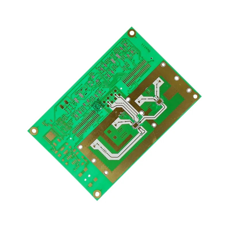
●Plate type: CEM-1, CEM-3 FR4, high TG material;
● Maximum board size: 600mm*700mm (24000mil*27500mil)
● Processing board thickness: 0.4mm-4.0mm (15.75mil-157.5mil)
●Maximum number of processing layers: 16Layers
●Copper foil layer thickness: 0.5-4.0(oz)
● Finished plate thickness tolerance: +/-0.1mm (4mil)
● Molding dimensional tolerance: Computer milling: 0.15mm (6mil) Mold punching: 0.10mm (4mil)
● Minimum line width/space: 0.1mm (4mil) Line width control capability: <+-20% ● Minimum drilling hole diameter of finished product: 0.25mm (10mil) Minimum punching hole diameter of finished product: 0.9mm (35mil) Finished product aperture tolerance: PTH: +-0.075mm (3mil) NPTH: +-0.05mm(2mil) ● Finished hole wall copper thickness: 18-25um (0.71-0.99mil) ● Minimum SMT patch spacing: 0.15mm (6mil) ●Surface coating: chemical immersion gold, spray tin, whole plate nickel gold plating (water/soft gold), screen printing blue glue, etc. ● Solder mask thickness on the board: 10-30μm (0.4-1.2mil) ● Peel strength: 1.5N/mm (59N/mil) ● Solder mask hardness: >5H
● Solder mask hole capability: 0.3-0.8mm (12mil-30mil)
● Dielectric constant: ε= 2.1-10.0
● Insulation resistance: 10KΩ-20MΩ
●Characteristic impedance: 60 ohm±10%
● Thermal shock: 288℃, 10 sec
● Warpage of finished board: <0.7%
● Product applications: communication equipment, automotive electronics, instrumentation, global positioning systems, computers, MP4, power supplies, home appliances, etc.

