How to determine the step of blind and buried vias? How to judge accurately?
PCB blind buried vias are a common type of vias on PCB boards and are also a widely used process in circuit board manufacturing. But what are the step of blind and buried vias? How to judge accurately?
1. What are PCB blind and buried vias?
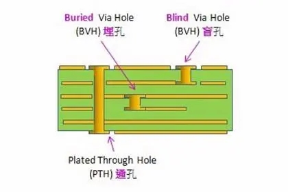
PCB blind buried vias are a type of via that connects the inner layer traces of the PCB to the surface traces. Blind vias and buried vias are two forms of blind and buried vias in PCB. A blind hole is a kind of via that only connects the inner layer and the surface layer. It needs to reserve a certain depth to facilitate the connection. It can be regarded as a kind of via hole of the inner layer pad. The buried via only connects the inner layer traces inside the PCB. It has nothing to do with the PCB surface traces and is usually used for multi-layer PCBs.
2. Definition of step of PCB blind and buried vias
According to the depth of blind holes or buried holes, blind holes or buried holes can be divided into different orders. First order means that one end of the blind hole can be seen, but the other end cannot be seen. The second level refers to a blind hole where neither end can be seen, but the length can be measured with a tool. At the third level, the length of blind holes and buried holes cannot be seen at all, and the length can only be determined by X-ray measurement.
3. How to accurately determine the step of blind and buried holes in PCB
Accurately judging the order of PCB blind and buried holes requires the use of professional instruments and tools for measurement. Commonly used measurement tools include: high-definition microscopes, solder needles, microscopes, and X-ray inspections. Among them, a high-definition microscope is the most basic tool, which can clearly observe blind holes or buried holes. Solder pins can be inserted into blind holes or buried holes to measure their depth. The microscope is suitable for observing blind and buried holes on complex PCB boards, and X-ray inspection is the most intuitive method, which can clearly observe the internal conditions of blind holes or buried holes.
4. The importance of blind and buried vias in PCB
PCB blind and buried vias are closely related to the electrical performance and reliability of PCB. The connection between the inner layer and the surface layer of the PCB is completed through blind holes. The connection quality of the blind hole well reflects the connection quality between the inner layer and the surface layer. If the order of blind holes is incorrect, it will lead to problems such as poor connections or separation of inner and surface traces, thus affecting the electrical performance and reliability of the PCB. Therefore, it is very important to judge the order of PCB blind and buried vias. Professional measurement tools and detection methods should be reasonably selected to ensure the quality of PCB blind and buried vias.
As an important part of PCB, PCB blind and buried vias directly affect the electrical performance and reliability of PCB. Accurately determining the order of blind and buried vias is very important for the PCB manufacturing process. Reasonable selection of professional measurement tools and detection methods can help us accurately judge PCB blind and buried vias and ensure the reliability and electrical performance of PCB.


