The past and present of printed circuit board
Printed circuit boards (PCBs) can be seen everywhere in life, ranging from Bluetooth headsets, electronic watches, calculators, to computers, communication equipment, military/aerospace systems. Wherever integrated circuits are needed, PCBs are inseparable from carrying electronic devices.
Before the advent of PCBs, electronic components were directly connected with wires. For equipment that used a large amount of components, the wiring was often messy, posing great safety hazards and prone to errors.

The emergence of PCB
In 1925, Charles Ducas of the United States printed a circuit pattern on an insulating substrate, and then used electroplating to successfully establish conductors for wiring. This method made it easier to manufacture electrical appliances. This is where the technical term “PCB” comes from.
In 1936, Austrian Dr. Paul Eisler published foil technology in the UK. He used printed circuit boards in a radio device. Also in 1936, Japan’s Miyamoto Kinosuke successfully applied for a patent for the spray-on wiring method. Of the two, Paul Eisler’s method is most similar to today’s printed circuit boards. This method is called the subtractive method, which removes unnecessary metal. The approach of Charles Ducas and Miyamoto Kinosuke is to add only the required wiring, which is called the additive method. Paul Eisler is also known as the “Father of Printed Circuits”. However, because the electronic tube components at that time generated a lot of heat, were bulky, and were inconvenient to install on printed circuit boards, this important invention of Paul Eisler was not taken seriously by the British at that time. , and in the United States, PCB manufacturing technology is only used in military products.
In 1942, Dr. Paul Eisler continued to improve his PCB production method and invented the world’s first practical double-sided PCB, which was officially produced at Pye Company. The patent application was approved in 1943. Around 1943, the United States began to use Paul Eisler’s technological invention on a large scale to create proximity fuses for use in World War II, using printed circuits as proximity fuses on bombs to act as bombs when they were close to the intended target. explosion timing device. At the same time, this technology is widely used in military radios.
In 1947, epoxy resin began to be used as a manufacturing substrate. At the same time, NBS began to research manufacturing technologies such as coils, capacitors, and resistors using printed circuit technology.
In 1948, the United States officially recognized the printed circuit board invention for commercial use.
Development of PCB
From the 1950s to the 1990s. This is the stage when the PCB industry was formed and grew rapidly, that is, the early stage of PCB industrialization. At this time, PCB has become an industry.
After 1948, the United States officially recognized the invention of PCB for commercial use, which also meant that PCB began to be commercialized on a large scale from military use. With the development of electronic technology, in December 1947, a research team composed of Shockley, Bardeen and Bratton at Bell Labs in the United States developed the transistor. Transistors with lower heat generation and smaller size began to replace them in large numbers in the 1950s. The status of electronic tubes has also created conditions for the widespread use of printed circuit board technology.
In 1950, a Japanese company tried coating silver on a glass substrate as a conductor and using copper foil on a phenolic resin paper substrate. Beginning in the 1950s, printed circuit manufacturing techniques became widely accepted, with etching playing a leading role. As transistors began to become practical, single-sided PCBs made by metal foil etching were successfully developed in the United States and quickly gained industrial application.
In 1951, polyimide material was born.
In 1953, Motorola developed a double-sided panel using the electroplated via method. Around 1955, Japan’s Toshiba Corporation introduced a technology to generate copper oxide on the surface of copper foil, and copper clad laminates (CCL) appeared. Both technologies were later widely used in the manufacture of multilayer printed circuit boards, and they contributed to the emergence of multilayer printed circuit boards. Since then, multi-layer PCB has been widely used.
In the 1960s, 10 years after printed circuit boards were widely used, PCB technology became increasingly mature. Since the advent of Motorola’s double-sided panels, multi-layer printed circuit boards have begun to appear, which has increased the ratio of wiring to substrate area.
In the 1960s, multi-layer (4+layers) PCBs began to be produced. The electroplated through-hole metallized double-sided PCB has achieved mass production.
In the 1970s, multi-layer PCBs developed rapidly and continued to develop in the direction of high precision, high density, fine line holes, high reliability, low cost and automated continuous production to adapt to the pace of Moore’s Law. Although multi-layer PCBs began to develop rapidly in the 1970s, PCB design work at that time was still completed manually.
The maturity of PCB
In 1993, Paul T. Lin of Motorola applied for a patent for a package called BGA (ball grid array), which marked the beginning of organic packaging substrates.
In 1995, Panasonic developed BUM PCB manufacturing technology with the ALIVH (arbitrary interlayer via) structure. This also marks the beginning of PCB’s entry into the era of HDI high-density interconnection.
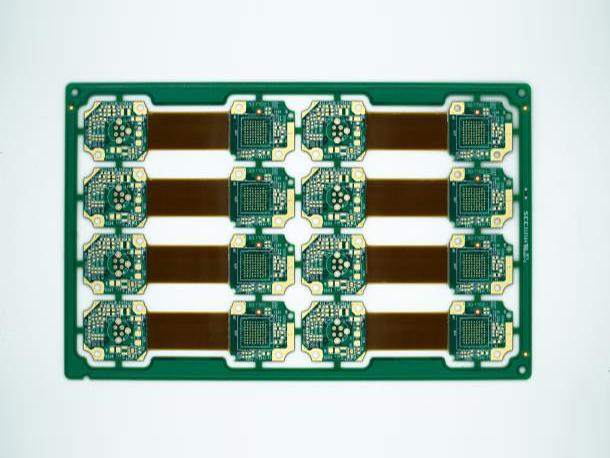
In the early 2000s, PCBs became smaller and more complex. 5-6 mil line width/line spacing is already a conventional process. For high-end PCB board manufacturers, they began to manufacture circuit boards with 3.5-4.5 mil line width/line spacing. At the same time, flexible PCBs became more common.
In 2006, the per-layer interconnect (ELIC) process was developed. The process uses stacks of copper to fill microvias to make connections through each layer of the circuit board. This unique process enables developers to create stacked connections between any two layers in a PCB. While this process increased the level of flexibility, allowing designers to maximize interconnect density, it was not until the 2010s that ELIC PCBs became widely used.
With the development of smartphones, it is driving the development of HDI PCB technology. At the beginning of the 21st century, while retaining laser-drilled micro-vias, stacked vias began to replace staggered vias, and combined with “any layer” construction technology, the final line width/line spacing of HDI boards reached 40μm. This arbitrary layer approach is still based on a subtractive process, and it is certain that most high-end HDI still uses this technology for mobile electronics. However, in 2017, HDI began to enter a new stage of development and began to shift from a subtractive process to a process based on pattern plating.
The future of PCBs
HDI and micropores provide a huge boost to high density due to miniaturization. These technologies will continue to evolve as IC cell geometries become smaller. So the next revolution will be in the field of optical conductors.
With the continuous improvement of VLSI technology, the performance of processors in computer systems has improved. However, electronic computers still use traditional copper wires to realize chip-chip, processor-processor, circuit board-circuit board connections. Connection, the International Technology Roadmap for Semiconductors (ITRS) has pointed out that future electronic systems will be limited by the interconnection between chips, because the main problems faced by the currently mainly used copper wires are: (1) high-speed signal distortion and limited bandwidth; (2) The transmission loss of metal wires increases with the increase of signal frequency, limiting the transmission distance of high-frequency signals; (3) Susceptible to electromagnetic interference; (4) High power consumption, etc.
Optical communication has many advantages that traditional electrical signals do not have, such as high bandwidth, low loss, no crosstalk, resistance to electromagnetic interference, etc. In fact, optical fibers have completely replaced traditional copper wires for long-distance communications for decades. The future development trend is that the communication distance of optical interconnections will gradually become shorter, from long-distance communications between countries to future chips. Internal signal transmission.
At present, the industry generally believes that when the single-channel rate reaches above 25Gb/s, electrical interconnection will face great challenges in terms of technical implementation and cost. Therefore, in order to overcome the “bottleneck” of electronic computers, we must change the traditional copper wire-based interconnection method, introduce optical technology into electronic systems, and replace traditional electrical interconnections with new optical interconnections. It will significantly increase the running speed of computers and promote the development of high-speed information communication networks, thereby meeting the needs of social development.

