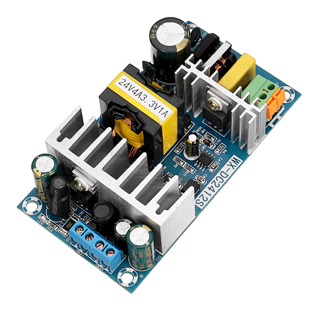
Refined PCB design of low-power DC-DC power module.
(1) Introduction to DC-DC power supply applications
1. Introduction to DC-DC application types
DC-DC power supply is the core device for DC voltage conversion, including LDO and other types. Among them, devices implemented using switching methods are often called DC-DC converters. This type of power supply has the advantages of low power consumption, high efficiency, small size, light weight, high reliability, anti-interference, and wide range output, so it is widely used in the electronic field.
2.Working principle of DC-DC power supply
The working principle of DC-DC power supply involves voltage conversion and regulation. This process is mainly realized through the converter of switching power supply. The DC-DC converter is responsible for converting the input DC voltage into the required output DC voltage in the switching power supply. In general, the working principle of this converter can be divided into three main steps:
1) Filtering: When the mains power is turned on through the input switch, it first becomes pulsating DC through the rectifier circuit, and then filters out the ripples through the filter circuit, turning it into smooth DC, which is supplied to the converter for conversion.
2) Conversion: The DC-DC converter generates a certain pulse power from the input voltage through the power switch tube and energy storage inductor, and then uses the pulse transformer and rectifier filter circuit to obtain the corresponding output voltage. The voltage conversion is achieved by controlling the switching timing of the switching tube through PWM (Pulse Width Modulation) or PFM (Frequency Modulation). In the switching power supply, the switching speed of the switching tube is very fast, and the switching action is generally completed within tens of microseconds. This speed is much faster than the adjustment speed of the traditional linear power supply.
3) Regulation: The stability of the output voltage is achieved through a feedback loop. When the output voltage increases, the sample signal obtained through the sampling resistor will increase. The error signal obtained after comparing this signal with the reference voltage will increase, and then the conduction of the switching tube is reduced through PWM or PFM control. The turn-on time is reduced, thereby reducing the average power output by the converter and achieving stability of the output voltage.
(2). Selection of key components
1. Output inductor
The inductor stores magnetic energy to ensure stable current output. When choosing an inductor, you need to weigh the size. Large inductors have small losses but slow response, while small inductors respond quickly but have large losses. Consider the saturation current to ensure the filtering effect.
2. Voltage dividing resistor
The voltage dividing resistors form a voltage dividing network and feed back the output voltage to the control circuit to accurately control the PWM duty cycle and stabilize the output voltage value. Choose high-precision resistors to ensure circuit accuracy.
3. Input capacitor
When selecting the input capacitor, consider the equivalent inductance and self-resonant frequency. Capacitors with large capacitance filter out low-frequency noise, and capacitors with small capacitance filter out high-frequency noise. Combination and parallel use can achieve excellent filtering effect, stabilize the input voltage and filter out AC components.
4. Output capacitor
The output capacitor filters out switching ripple and ensures pure output current. The larger the capacitance, the smaller the impedance and the easier it is for ripples to flow through. Choosing the appropriate output capacitor is critical to the stable operation of the circuit.
When selecting these core components, we need to consider various factors to achieve the best balance. For example, the selection of the inductor requires a balance between efficiency and response speed; the voltage divider resistor needs to accurately and stably feedback the voltage; the input and output capacitors need to be selected according to different operating frequency noise characteristics; and the final output capacitor needs to be Consider capacitance and ESR to minimize ripple. Through careful selection, we can make the circuit work in an efficient and stable state, thereby maximizing the performance of the circuit.
(3)DC-DC power supply layout and wiring recommendations
For power module layout and wiring, you can download the chip’s datasheet in advance and design according to the recommended layout and wiring.
1. Layout design
1) Chip power supply proximity principle: For the switching power supply that provides voltage to the chip, ensure that it is placed as close to the chip as possible. This prevents low-voltage output lines from being too long, thereby reducing voltage drop and ensuring that power supply performance is not affected.
2) Avoid electromagnetic interference: Switching power supplies work under high voltage and large current conditions, which may cause complex electromagnetic compatibility issues. Therefore, sensitive components should be avoided around the switching power supply to reduce the impact of electromagnetic interference on the work of the components.
3) Layout with the power supply chip as the core: During layout, the switching power supply chip should be organized as the core component. The input and output ends of the power filter should be laid out to ensure sufficient distance to prevent noise from coupling from the input end to the output end. Components should be arranged neatly and compactly on the PCB to reduce and shorten the leads and connections between components.
2. Wiring design
1) Avoid parallel wires: The wires used at the input and output ends should avoid adjacent parallel wires as much as possible to reduce unnecessary electromagnetic interference.
2) Thick ground wire: Thickening the ground wire between the input and output can ensure stable current and reduce feedback coupling.
3) Handling of high-current leads: High-current leads, such as public ground wires, power input/output wires, etc., should be made as thick as possible. This can reduce wiring resistance and voltage drop, thereby reducing self-excitation caused by parasitic coupling.
3. Heat dissipation considerations
1) Heat dissipation ground area: Since the heat dissipation of the switching power supply is relatively large, the area of the heat dissipation ground (copper) should be increased as much as possible to ensure effective heat dissipation.
2) Large-area copper laying and drilling: The input and output ends should be laid with copper over a large area and drilled with as many holes as possible. This can not only meet the current requirements, but also help improve the heat dissipation effect.

