PCB wiring rules: What are the connector connection methods?
Everyone knows about PCB, but do you know about its wiring? As an integral part of the whole machine, a PCB generally cannot constitute an electronic product, and there must be problems with external connections. For example, electrical connections are required between PCBs, between PCBs and off-board components, and between PCBs and equipment panels. PCB wiring can be said to be a basic course for every electronic engineer. The following is a brief analysis of the wiring of each PCB component for your reference.
In more complex instruments and equipment, plug-in connectors are often used. This “building block” structure not only ensures the quality of product mass production, reduces the cost of the system, but also provides convenience for debugging and maintenance. When equipment fails, maintenance personnel do not have to check to the component level (that is, check the cause of the failure and trace it back to the specific components. This work takes a lot of time), as long as they determine which board is abnormal. It can be replaced immediately, troubleshooting in the shortest possible time, shortening downtime and improving equipment utilization. The replaced circuit board can be repaired in ample time and used as spare parts after repair.
1. Standard pin connection
This method can be used for external connection of PCB, especially in small instruments, pin connection is often used. Two PCBs are connected through standard pins. The two PCBs are generally parallel or vertical, making it easy to achieve mass production.
2. PCB socket
This method is to make a printed plug from the edge of the PCB. The plug part is designed according to the size of the socket, the number of contacts, the contact distance, the position of the positioning holes, etc., so that it matches the dedicated PCB socket.
When making boards, the plug part needs to be gold-plated to improve wear resistance and reduce contact resistance. This method has simple assembly, good interchangeability and maintenance performance, and is suitable for standardized mass production. The disadvantage is that the PCB cost increases, and the PCB manufacturing accuracy and process requirements are higher; the reliability is slightly poor, and poor contact is often caused by the oxidation of the plug part or the aging of the socket reed. In order to improve the reliability of external connections, the same lead wire is often led out in parallel through the contacts on the same side or both sides of the circuit board.
PCB socket connection methods are often used in products with multi-board structures. There are two types of sockets and PCB or base plates: reed type and pin type.
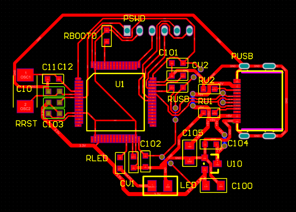
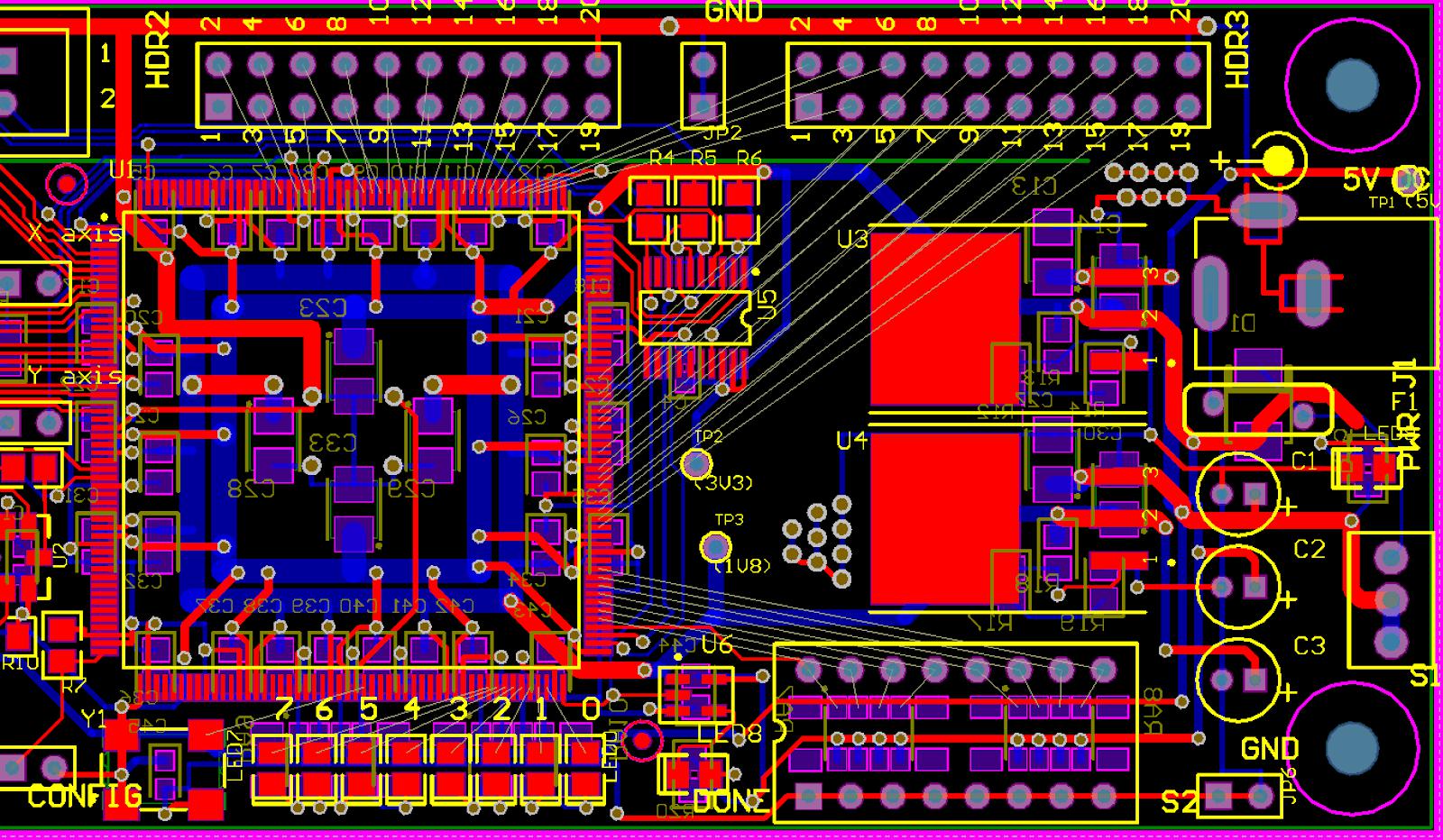
PCB wiring rules
1. Cross circuits are not allowed in printed circuits. For lines that may cross, “drilling” and “winding” can be used to solve them. That is, let a certain lead “drill” through the gap at the foot of other resistors, capacitors, and transistors, or “wind” through one end of a lead that may cross. In special cases, the circuit is very complicated. To simplify the design, Wire jumpers are allowed to solve cross-circuit problems.
2. Resistors, diodes, tubular capacitors and other components can be installed in two ways: “vertical” and “horizontal”. The vertical type means that the component body is installed and welded perpendicularly to the circuit board. Its advantage is that it saves space. The horizontal type means that the component body is installed and welded parallel and close to the circuit board. Its advantage is that the mechanical strength of the component installation is better. For these two different mounting components, the component hole spacing on the printed circuit board is different.
3. The grounding points of circuits of the same level should be as close as possible, and the power supply filter capacitor of this level of circuit should also be connected to the grounding point of this level. In particular, the grounding points of the base and emitter of the transistor of this level cannot be too far apart, otherwise interference and self-excitation will occur because the copper foil between the two grounding points is too long. A circuit using such a “one-point grounding method” will work more slowly. Stable and not prone to self-excitation.
4. The general ground wire must be strictly arranged according to the principle of high frequency-medium frequency-low frequency in the order of weak current to strong current. It must not be randomly connected over and over again. It is better to have longer wiring between levels. Follow this rule. In particular, the requirements for the grounding wire arrangement of the frequency converter head, regeneration head, and frequency modulation head are more stringent. If there is any improper grounding wire arrangement, self-excitation will occur and the grounding wire will not work. High-frequency circuits such as FM heads often use large-area surrounding ground wires to ensure good shielding effects.
5. High-current leads (public ground wires, power amplifier power leads, etc.) should be as wide as possible to reduce wiring resistance and voltage drop, and reduce self-excitation caused by parasitic coupling.
6. Keep high-impedance traces as short as possible, and low-impedance traces as long as possible, because high-impedance traces tend to emit and absorb signals, causing circuit instability. The power wire, ground wire, base wire of non-feedback components, emitter wire, etc. are all low-impedance wires. The base wire of the emitter follower and the ground wires of the two channels of the radio must be separated and formed into a separate path. , until the end of the function and then combined together. If the two ground wires are connected back and forth, it is easy to produce crosstalk and reduce the separation.

