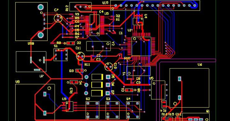
PCB wiring analog circuit and digital circuit part
Wiring features:
1. The placement direction of components determines the direction of wiring.
2. The wiring directions of adjacent layers are different. The wiring main body of the surface layer and the welding layer of the two panels is 90?3. The wiring direction of the rectangular circuit board is longitudinal. Horizontal wiring can easily cause congestion or even failure to wire.
4. Try to ensure the wiring space. When this is not possible, use specific components for wiring, and try to avoid connecting holes under the components.
Because when the circuit board fails, it is impossible to visually see the status of the connection holes under the components and whether they are short-circuited with other wiring or component pins.
Analog circuit part and digital circuit part
Including wiring, the analog circuit part and the digital circuit part must be kept above 5mm to ensure that there is no signal interference with each other.
When a symbol is used to represent a ground wire in a circuit diagram, the circuit board designer needs to analyze the circuit diagram and set a certain area. Power cords and ground wires were originally designed. For two-panel and four-layer boards, the wiring composition is completely different. Because the power supply and ground wires are set on the inner layer, attention is mainly focused on them. Just focus on the layout of the signal lines. For beginners, it is recommended to start with the design of four-layer boards. The wiring of power lines and ground wires has a great impact on electricity and noise, so they must be designed carefully.
Take two panels as an example:
○The power cord and ground wire are designed on the same layer, and the effect is very poor
○The ground wire is on the surface and the power wire is on the welding layer. General design
○The ground wire is on the surface, the power wire is on the welding layer, and is wired in copper foil, which has a better anti-clutter effect. Because of the uncontrollability of CAD design, the design takes longer than simple wiring. Pay attention to ensure a small wiring width to ensure that no disconnection or flow obstruction occurs.
To put it simply: the power cord and ground wire are equivalent to the aorta and veins of the human body. You can also simply think of water pipes. The wider the line width, the greater the current flow and faster heat dissipation. The narrower the line width, the greater the resistance under the same voltage, the smaller the current flow that can pass, and the slower the heat dissipation.
Surface welding surface
For power lines and ground wires, large-scale copper foil wiring is used.
Precautions for wiring power lines and ground wires on two-layer circuit boards
Normally, the power wire is routed on the welding surface, the ground wire is routed on the surface, and copper foil is used to wire a wide area, and then some more capacitance is added between the power wire and the ground wire, and there is basically no problem. But if electromagnetic interference is involved, the problem is different. When it exceeds 8MHz, problems of this kind may occur. When it exceeds 25MHz, it will become quite unstable. At this time, it is necessary to surround the important components with ground copper foil, and also design the ground copper foil on the soldering surface.
Crystal oscillator wiring
In order to resist interference, the components should be surrounded by ground copper foil as much as possible. What is not shown in the picture is that ground copper foil can also be laid under the crystal oscillator on the soldering layer, and then the surface and the soldering surface are connected with connection holes. Enhance anti-interference ability.
The use of thermal resistive pads
When power lines and ground wires are routed using large pieces of copper foil, they should be designed using heat-resistant pads as much as possible. This is because if the component pad is directly connected to a large piece of copper foil, the heat will dissipate quickly during welding, and the temperature of the melted solder will not be enough, resulting in poor welding or virtual soldering.
Thermal resistive pad
Power supply for analog circuits
The output part should be close to the power supply. In order to not be affected by the output part, the high-sensitivity input part must be kept at a certain distance from the output part.
Analog circuit diagram Schematic diagram of the separation of digital circuit and analog circuit parts Power input part
DC power supply: When power is provided from the outside, it must first pass through the electrolytic capacitor and then be provided to the internal circuit. The wiring method is usually as follows.
The two-layer panel provides power to the internal circuit not through point A, but through point B. The multi-layer panel also introduces power to the inner layer after passing point B.


