Enhance product performance! The strong competitive advantage brought by multi-layer PCB lamination process!
As technology continues to advance, the demand for electronic products is also growing. In order to meet consumer requirements for higher performance and smaller size, the multi-layer PCB lamination process has become a key link in the design of modern electronic products.
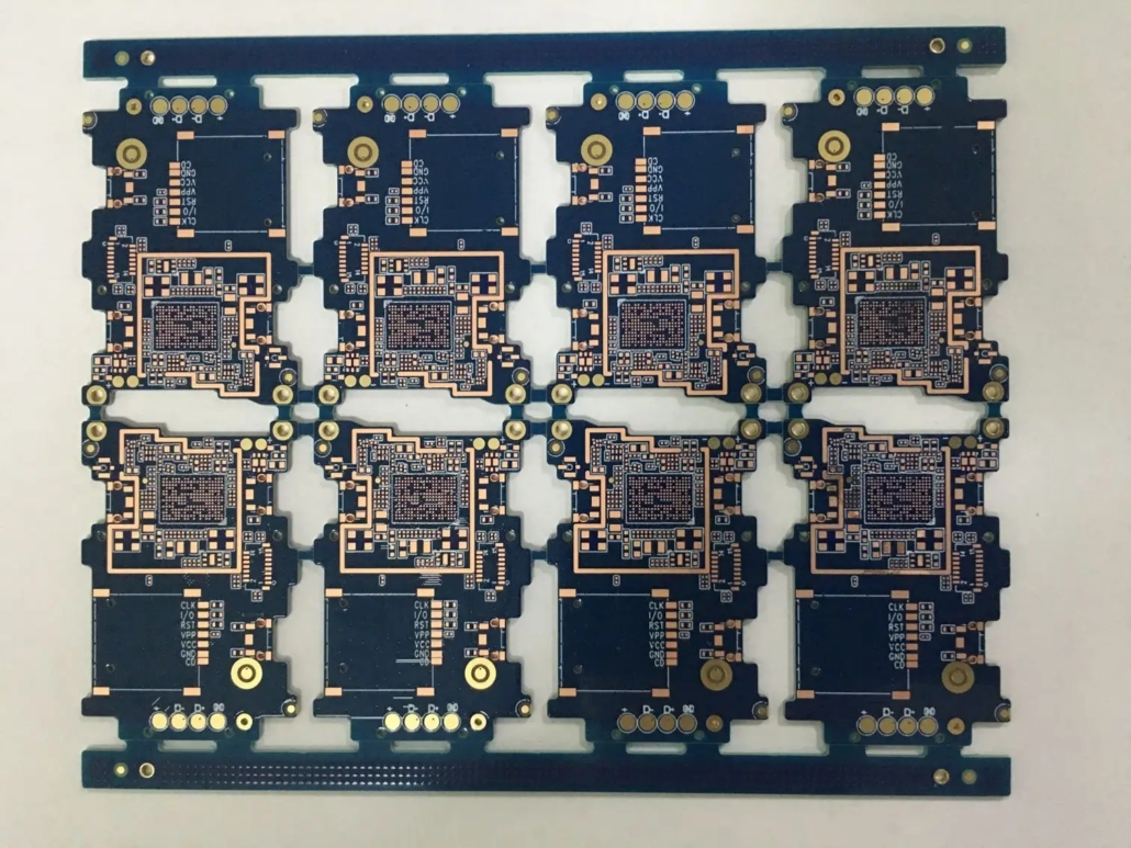
Multi-layer PCB lamination process can provide higher circuit density. Compared with traditional single-layer circuit boards, multi-layer PCBs can accommodate more electronic components and connection lines, thereby achieving more complex functional integration. This is critical for modern electronics, which often require more functionality and performance in a limited space.
The multi-layer PCB lamination process can also improve the stability and reliability of the circuit. Since the multi-layer PCB adopts a stacked design, the connections between electronic components are closer, reducing interference and loss in signal transmission. In addition, multi-layer PCBs also have better anti-interference performance and can effectively resist external electromagnetic interference and noise. These characteristics make multi-layer PCBs perform well in application fields such as high frequency and high-speed transmission.
In addition, the multi-layer PCB lamination process can also improve the heat dissipation performance of the product. As the power consumption of electronic products increases, heat dissipation issues have become an important factor restricting product performance. The stacking design of multi-layer PCB can effectively improve the heat dissipation effect. Through reasonable thermal conduction design and heat dissipation channels, heat is quickly conducted to the external environment and the normal operating temperature of electronic components is maintained, thereby improving the stability and life of the product.
The multi-layer PCB lamination process can also simplify the product manufacturing process. Compared with using multiple single-layer circuit boards for assembly, multi-layer PCBs can directly weld electronic components to different levels of circuit boards, reducing the use of connecting wires, simplifying the assembly process, and improving production efficiency. This is especially important for large-scale production and fast delivery requirements.
In the electronics industry, mastering the design and manufacturing technology of multi-layer PCB lamination process will bring greater market competitiveness to enterprises. Therefore, we should pay attention to the application and development of multi-layer PCB lamination technology and continuously promote the enhancement of product performance to meet users’ needs for high-quality electronic products.

