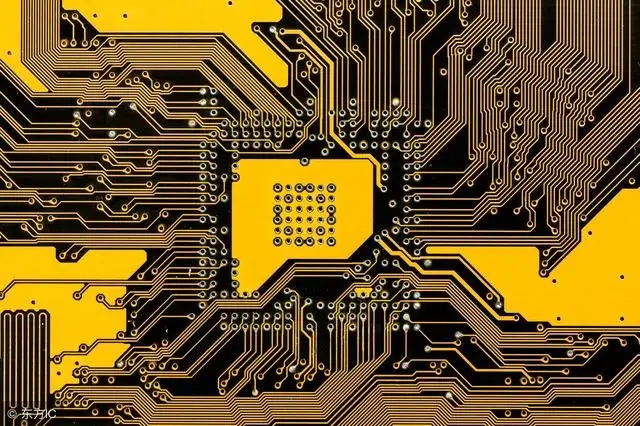
Learn about impedance board control technology and easily improve PCB signal transmission efficiency!
Impedance PCB control technology can effectively improve PCB signal transmission efficiency, reduce signal interference, and ensure the reliability of data transmission.
1. The concept and function of impedance PCB
The impedance PCB refers to the geometric shape of the circuit board on the PCB, which is used to control the impedance matching of signals during PCB transmission. Impedance matching means that the impedance between the source and terminal is the same, so that neither the signal is reflected nor the signal is lost. In high-speed data transmission, the signal frequency is high, the signal waveform is seriously deformed, and signal reflection and signal loss are prone to occur, thus reducing the signal transmission efficiency. Therefore, the design of the impedance board is very important, which can help us control the impedance matching of the signal, reduce signal loss and reflection, and improve the reliability of signal transmission.
2. Design of impedance PCB
The design of the impedance PCB needs to consider board thickness, board dielectric constant, line width and distance, and the number of wiring layers. The larger the thickness of the board and the thinner the line width, the impedance of the signal will also increase; the larger the dielectric constant of the board, the impedance will also increase accordingly; the smaller the line spacing can also increase the impedance. Through the design of these parameters, the impedance of the signal can be effectively controlled and the stability of signal transmission can be improved.
3. Optimization of impedance PCB
The optimization of the impedance PCB mainly includes three aspects: trace layout, line width and line spacing optimization, and location optimization. In actual applications, the layout of the circuit board also has a great impact on impedance matching, so some optimization needs to be done. In terms of wiring layout, design principles such as focusing on route length, avoiding right-angle lines, and avoiding side-by-side lines can be adopted; for optimization of line width and line spacing, technologies such as microstrip lines and coaxial cables can be considered to make the signal impedance close to 50Ω. In addition, designers need to optimize the impedance plate through electromagnetic field simulation analysis.
4. Detection and diagnosis of impedance PCB
During the PCB manufacturing process, the impedance board also needs to be tested and diagnosed to ensure the accuracy of the impedance parameters. The main detection methods include self-test method, inter-board test method, and time domain reflection method. At the same time, once an impedance mismatch is discovered, it needs to be resolved promptly.
Impedance board control technology is an important method to improve PCB signal transmission efficiency and reduce signal interference. By designing and optimizing the impedance plate, signal loss and reflection can be reduced and the reliability of signal transmission can be improved. At the same time, the accuracy of the impedance parameters is ensured through the detection and diagnosis of the impedance PCB. Impedance plate control technology is an indispensable part of circuit design.

