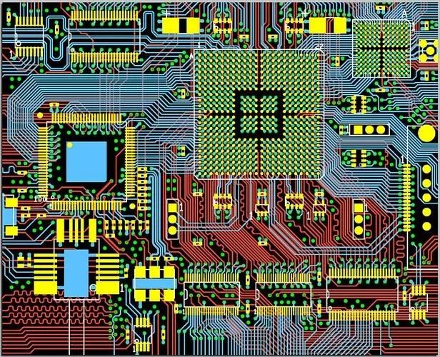
Layout and routing of PCB components.
PCB design is 90% in device layout and 10% in wiring. If the PCB is designed well, it can get twice the result with half the effort and also improve the electrical characteristics of the PCB.
For example, if you want to improve work efficiency, you need to pay attention to the space for wiring to prevent re-routing due to lack of space; or if you don’t want to find that it cannot be soldered when soldering the board, you need to pay attention to the placement of components and consider the edges of the board. Distance and other factors; and if you want a PCB board that looks good and is easy to debug, you need to pay more attention to the overall layout of the PCB. These must be planned in advance to make the PCB board symmetrical, clean and beautiful.
Of course, for the same circuit diagram, 100 electronic engineers will have 1,000 wiring schemes. Because designing a circuit board is also a process of artistic creation, and different people have different aesthetic standards, so we do not define fixed PCB layout wiring standards. But I will provide you with a basic idea, based on which designers can design the most beautiful PCB board in their mind.
PCB layout tips
1. Understand the physical limitations of the circuit board
Before placing components, determine the mounting holes of the circuit board, the location of edge connectors, and the mechanical size constraints of the circuit board.
2. Understand the circuit board manufacturing process
The assembly process and testing process of the circuit, whether it is necessary to reserve space for the PCB V-shaped groove, the component welding process, etc.
3. Leave breathing space for integrated chips
When placing components, try to leave at least 350mil between them. For chips with many pins, the space needs to be larger.
4. The same device has the same direction
For identical devices, keep the formation as consistent as possible. It facilitates the later assembly, inspection and testing of circuit boards and ensures consistent high solder joints.
5. Reduce lead crossings
Reduce lead crossings by adjusting device position and orientation. It can save a lot of effort for later wiring.
6. Place circuit edge components first
For devices that cannot be moved arbitrarily due to mechanical restrictions, they must be placed first, such as external connectors, switches, USB ports, etc. on the circuit board.
7. Avoid conflicts between devices
Absolutely avoid overlapping and sharing the pads of devices or overlapping the edges of devices in order to route them in a small circuit board. It is best to maintain a distance of 40mil between all devices.
8. Place the devices on the same side as much as possible
The devices on the circuit board are completed by an automatic device placement machine. The devices are only on one side. The PCB production process only needs one pass. Otherwise, the devices will be placed twice, which wastes production time and costs.
9. Keep the polarity of chip pins and devices consistent
If the polarity and orientation of the components on the circuit board are messy, it will hinder the successful soldering of the circuit board.
10. The device location is similar to that on the schematic diagram
When designing the schematic diagram, the positional relationship between the devices has been optimized (the shortest connections and the least crossovers), so it will be more reasonable to place the PCB devices according to the device positions on the schematic diagram.
PCB routing rules
1. Routing direction control rules
That is, the wiring directions of adjacent layers form an orthogonal structure. Avoid running different signal lines in the same direction on adjacent layers to reduce unnecessary inter-layer interference; when it is difficult to avoid this situation due to board structure limitations (such as some backplanes), especially when the signal rate is high, Consider using ground planes to isolate wiring layers and ground signal lines to isolate signal lines.
2. Open-loop inspection rules for wiring
Generally, wiring with one end floating (Dangling Line) is not allowed, mainly to avoid the “antenna effect” and reduce unnecessary interference radiation and reception, otherwise it may bring unpredictable results.
3. Impedance matching check rules
The wiring width of the same network should be consistent. Changes in line width will cause uneven line characteristic impedance. When the transmission speed is high, reflection will occur. This situation should be avoided in the design.
4. Trace length control rules
That is, the short line rule. When designing, the wiring length should be kept as short as possible to reduce interference problems caused by too long wiring. Especially for some important signal lines, such as clock lines, the oscillator must be placed very close to the device. The place.
5. Chamfering rules
Sharp angles and right angles should be avoided in PCB design, which will produce unnecessary radiation and poor process performance.
6. Device decoupling rules
Add necessary decoupling capacitors to the printed plate to filter out interference signals on the power supply and stabilize the power supply signal.
7. Ground loop rules
The minimum loop rule means that the loop area formed by the signal line and its loop should be as small as possible. The smaller the loop area, the less external radiation and the smaller the external interference received.
8. Integrity rules for power and ground layers
For areas with dense via holes, care should be taken to avoid the holes connecting to each other in the hollowed-out areas of the power supply and ground layers, forming a division of the plane layer, thereby destroying the integrity of the plane layer, and thereby causing an increase in the loop area of the signal line in the ground layer. .
9. Shielding protection
The corresponding ground loop rule is actually to minimize the loop area of the signal, which is more common in some more important signals, such as clock signals and synchronization signals.
10. Cabling closed-loop inspection rules
Prevent signal lines from forming self-loops between different layers. Such problems are prone to occur in multilayer board designs, and self-loops will cause radiated interference.
11. Isolated copper zone control rules
The emergence of isolated copper areas will bring about some unpredictable problems. Therefore, connecting the isolated copper areas with other signals will help improve the signal quality. Usually, the isolated copper areas are grounded or deleted.

