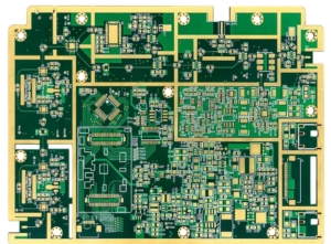
How to understand the minimum rules for PCB line spacing and hole spacing?
With the trend of miniaturization and complexity of modern electronic devices, the accuracy and rationality of the design of PCB printed circuit boards as a connecting bridge between electronic components are particularly important. The design of PCB is not only related to the stable performance of the product, but also directly affects the manufacturing cost and production efficiency. Among the many design rules, the minimum setting of PCB line spacing (the distance between line widths) and hole spacing (the distance from the edge of the hole to the adjacent wire) is one of the key factors to ensure the normal operation of the circuit, avoid short circuits and improve the success rate of manufacturing.
Overview of PCB line spacing and hole spacing PCB line spacing refers to the minimum allowable distance between the center lines of any two conductive lines on the PCB. This distance must be large enough to prevent accidental electrical connections (i.e. short circuits) caused by damage to insulating materials during the manufacturing process or when the circuit is running. The size of the line spacing is affected by many factors such as the materials used, manufacturing process, operating voltage, expected current, and expected working environment.
Hole spacing refers to the minimum allowable distance from the edge of the hole (via used to install component pins or realize interlayer connection) on the PCB to the edge of the nearest wire. Reasonable hole spacing design can ensure that the drilling and copper plating process will not damage the adjacent wires, while reducing the crosstalk between signals and ensuring the signal integrity of the circuit.
Why is the minimum spacing rule established?
1. Electrical safety: Too small line spacing and hole spacing may cause current leakage, causing short circuits, and in severe cases, damage the circuit board or even the entire system.
2. Manufacturing feasibility: Different manufacturing processes have their technical limitations, such as etching accuracy, drilling accuracy, etc. Too small spacing will increase the difficulty of manufacturing and reduce the yield rate.
3. Signal integrity: Electromagnetic interference is easily generated between conductors that are too close, affecting the quality of signal transmission, causing signal attenuation, delay or distortion.
4. Thermal management: Dense layout may hinder heat dissipation and affect the long-term reliability and life of components.
Factors affecting the minimum spacing Circuit operating voltage and current: High voltage or high current circuits require larger line spacing to reduce the risk of breakdown. Signal frequency: High-frequency signals are more sensitive to line spacing to reduce crosstalk and ensure signal quality. Manufacturing process: Advanced manufacturing technology can support smaller line spacing and hole spacing, but the cost increases accordingly. Environmental factors: such as temperature cycling, humidity, etc., require more conservative designs to improve reliability in harsh environments.
Design practice recommendations Follow manufacturer guidelines: Each PCB manufacturer will provide specific manufacturing capability parameters, including minimum line spacing and hole spacing requirements, which must be strictly followed during design. Use design software assistance: Modern PCB design software usually has a built-in DRC (design rule check) function to help designers automatically detect and adjust line spacing and hole spacing that do not meet specifications. Reserve margin: Under the premise of meeting performance requirements, appropriately increase line spacing and hole spacing to leave room for manufacturing tolerances and potential design modifications. Multilayer board design considerations: For multilayer boards, it is also necessary to consider the impact of inter-layer alignment and via penetration on adjacent layers for comprehensive design.
In short, the line spacing and hole spacing of PCBs are one of the most basic and critical design elements, which are directly related to the performance, reliability and manufacturing cost of the circuit board. By deeply understanding these rules and combining specific project requirements and manufacturing capabilities, designers can effectively avoid common design errors and create electronic products that are both efficient and reliable.


