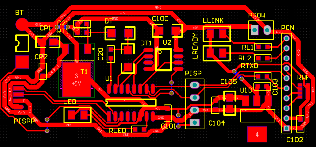
How to quickly find GND in PCB?
In the PCB design and production process, finding the ground wire (GND) is a very critical step. GND is a very important reference plane in electronic circuits. It provides a reference level in the circuit and provides a low-noise current path in the circuit. Therefore, finding GND accurately is key to ensuring the circuit works properly. In the following article, we will detail how to quickly find GND in a PCB.
1. GND planning in the PCB design stage:
Before starting to design the PCB, you must first plan the GND. This requires designers to consider the layout of GND during the schematic and layout stages to ensure that the entire circuit is properly laid out on the PCB. When planning GND, there are some principles:
– Try to keep the GND line short and straight. Do not allow GND current to pass through signal lines or other high-frequency lines.
– Minimize the area of the GND loop. A large GND loop will form an antenna and introduce electromagnetic radiation or interference.
– The ground trace opposite the high power source should be wide enough to ensure good current flow throughout the PCB.
– Take care to split the GND into different areas to avoid current interference between different parts.
2. Use a ground plane layer:
The ground plane layer is the layer in the PCB used to form the GND reference plane. It serves to connect individual power pins and other circuit components by creating a continuous copper area between the top and bottom layers of the PCB. During the design process, we can do the following:
– Wrap the entire circuit layout around the ground plane layer, making sure there are no gaps around GND.
– Add GND station holes or GND copper posts near the power pins to strengthen the GND connection.
– Try to use multi-layer boards and use the inner grid layer and ground plane layer to provide a better GND connection.
3. Use GND pin:
On some devices such as power supplies and amplifiers, there will be a dedicated GND pin that is directly connected to the GND reference plane. Properly connecting these pins to the GND plane can help reduce GND voltage drop and noise.
4. Use the remaining electronic connection points:
In some complex circuits, there may be some remaining unused electrical connection points. These connection points are often called electrically sensitive points (ESD). Connecting these connection points to GND can help reduce interference with the circuit.
5. Use the ground test tool:
After the PCB is produced, we can use some ground test tools to confirm the GND connection. These tools can verify GND connectivity by checking that the current flow on the ground wire is smooth and normal.
To sum up, to quickly find the GND in the PCB, we need to carry out reasonable GND planning at the design stage, use the ground plane layer and GND pin to provide a reliable GND connection, and use the remaining electronic connection points and ground test tools to ensure GND for connectivity and reduced interference. Through reasonable design and testing, we can ensure that the GND connection in the PCB is correct and reliable, thereby ensuring the normal operation of the entire circuit.

