How to check the quality of PCB circuit board after laser welding?
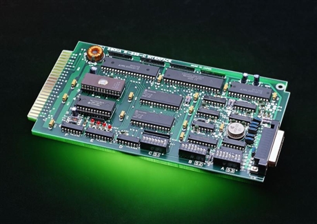
As 5G construction continues to advance, industrial fields such as precision microelectronics and aviation and shipbuilding have further developed, and these fields all cover the application of PCB circuit boards. With the continuous development of these microelectronics industries, we will find that the manufacturing of electronic components is gradually becoming miniaturized and thinner, and the requirements for precision are getting higher and higher. As the most commonly used processing technology in the microelectronics industry, laser welding is bound to There are increasingly higher requirements for the welding level of PCB circuit boards.
Inspection after PCB circuit board welding is very important for both enterprises and customers. In particular, many enterprises have strict requirements for electronic products. If inspection is not done, performance failures will easily occur, affecting product sales, corporate image and word of mouth. The laser welding equipment produced by Shenzhen Zichen Laser has fast efficiency, high welding yield, and post-weld inspection function, which can meet the welding processing and post-weld inspection needs of enterprises. So, how to check the quality of PCB circuit board after welding? Below Zichen Laser shares several commonly used detection methods.
01 PCB triangulation
What is triangulation? That is, the method used to check the three-dimensional shape. At present, the triangulation detection method has been developed and used and equipment capable of detecting its cross-sectional shape has been designed. However, because this triangulation detection method is incident from different lights and in different directions, the observation results will be different. Essentially, objects are inspected through the principle of light diffusion. This method is the most appropriate and most effective. As for the situation where the welding surface is close to mirror surface conditions, this method is inappropriate and difficult to meet production needs.
02 Light reflection distribution measurement method
This method mainly uses the welding part to detect the decoration, injects light inward from an oblique direction, sets a TV camera above, and then inspects it. The most important part of this operation method is how to know the surface angle of the PCB solder, especially how to know the irradiation photometric information. The angle information must be captured through various light colors. On the contrary, if it is illuminated from above, the angle measured is the reflected light distribution, and just check the tilted surface of the solder.
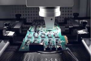
03 Change the angle for camera inspection
How to detect PCB after welding? To use this method to detect the quality of PCB after welding, a device with a changing angle is necessary. This device generally has at least 5 cameras, multiple LED lighting equipment, uses multiple images, and uses visual inspection conditions for inspection, so the reliability is relatively high.
04 Focus detection utilization method
For some high-density circuit boards, after PCB welding, the above three methods are difficult to detect the final result, so the fourth method, which is the focus detection and utilization method, needs to be used. This method is divided into multiple methods, such as the multi-stage focus method, which can directly detect the height of the solder surface and achieve high-precision detection. If 10 focus surface detectors are set up at the same time, the focus surface can be obtained by seeking the maximum output and detect The position of the solder surface. If it is detected by irradiating the object with a fine laser beam, a lead device with a pitch of 0.3mm can be successfully detected by staggering 10 specific pinholes in the Z direction.

