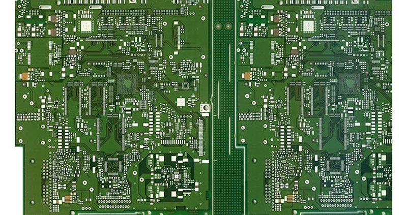
Differences between PCB positive and negative film processes.
PCB positive and negative films are two important steps in the PCB manufacturing process, and there are some differences between them. Below we will explore the flow of these two processes and their differences in detail.
First, let’s understand the concepts of positive and negative films. In PCB manufacturing, the photolithography process mainly involves the production of photographic plates. The positive film is usually used to make the copper layer pattern of the PCB, while the negative film is used to make the solder mask, character logo and other patterns of the PCB.
Feature film process:
1. Design drawing: First, use CAD software to make drawings according to the PCB design drawings, including wiring, component installation locations, solder mask areas, etc.
2. Make negatives: Convert the drawings into negatives suitable for PCB production, usually using translucent film for printing.
3. Prepare photosensitive coating: In order to allow the pattern on the negative film to be transferred to the PCB material, a layer of photosensitive coating needs to be applied to the PCB material.
4. Exposure and development: Place the negative film on the PCB material coated with photosensitive agent, and transfer the pattern on the negative film to the PCB material through the exposure machine. Then, the exposed PCB material is developed to remove the unexposed portion of the photosensitive coating, leaving the exposed portion.
5. Corrosion: Use chemicals to corrode the developed PCB material to remove the copper layer in the exposed area, leaving only wiring, pads and other required circuits.
6. Cleaning: Clean the corroded PCB to remove residual photosensitizer and corrosive agent.
7. Solder mask and character marking: According to the PCB design requirements, the PCB is processed with solder mask and character marking.
Negative process:
1. Design and drawing: Just like the positive film, you first need to design and draw, including patterns such as solder mask and character logos.
2. Make negatives: Convert the designed drawings into negatives suitable for PCB production.
3. Prepare the negative film: Place the negative film on a piece of ordinary negative film, and fit the two negative films together to ensure accurate positioning.
4. Exposure and development: Place the negative film on the PCB material coated with photosensitizer, and transfer the pattern on the negative film to the PCB material through the exposure machine. Then, the exposed PCB material is developed to remove the unexposed portion of the photosensitive coating, leaving the exposed portion.
5. Corrosion: Use chemicals to corrode the developed PCB material to remove the copper layer in the unexposed areas, leaving only wiring, pads and other required circuits.
6. Cleaning: Clean the corroded PCB to remove residual photosensitizer and corrosive agent.
7. Solder mask and character marking: According to the PCB design requirements, the PCB is processed with solder mask and character marking.
The main difference between the positive and negative processes is the way the negative is made and the direction in which the pattern is transferred during the exposure process. In the positive film process, making negatives is to directly convert the designed drawings into negatives suitable for PCB production. In the negative film process, a negative film needs to be made first, then laminated to an ordinary film, and the pattern on the negative film is transferred to the PCB material through exposure.
In addition, other steps in the positive and negative processes, such as preparing the photosensitive coating, developing, etching, cleaning, soldering mask and character marking, are the same.
To sum up, the process differences between positive films and negative films in the PCB manufacturing process are mainly reflected in the way of making negative films and the direction of pattern transfer during the exposure process. Positive film is to directly convert the designed drawings into negative film, while negative film requires making a negative film and laminating it with ordinary negative film. Other steps such as photosensitization, development, etching, cleaning and solder mask are the same. The difference between these two processes allows them to achieve different pattern requirements of PCB, thereby meeting different PCB design needs.


