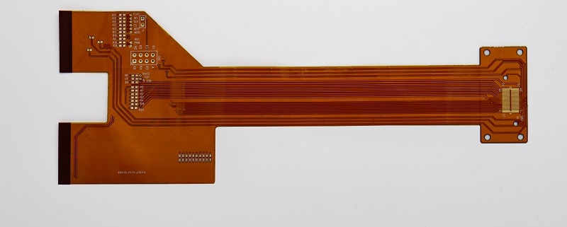
Flexible Printed Circuit Board (FPC) is a flexible electronic component that is widely used in various electronic devices. It is different from traditional rigid circuit boards. Its main feature is that it can be bent, folded and twisted to adapt to various complex shapes and space constraints. In the field of modern technology, FPC is used more and more widely. Today we will reveal the secrets of flexible circuit boards and quickly understand the various types and uses of FPC.
First, let us understand the basic structure of fpc. FPC consists of conductive layer, insulating layer and protective layer. The conductive layer is usually made of copper foil and is used to transmit current and signals. The insulating layer is made of materials such as flexible polyimide and serves to isolate the conductive layer. The protective layer is used to protect the FPC from the external environment, such as moisture, dust and mechanical damage.
According to different application requirements, FPC can be divided into many types.
Single-sided FPC is the simplest type, with only one conductive layer, so the wiring density is not high, but it has good flex resistance.
Double-sided FPC has conductive layers on both sides, which is suitable for some scenarios that require more complex circuit layouts, but its softness is worse than that of single-sided panels.
Multilayer FPC, which has multiple conductive layers embedded inside, is suitable for more complex electronic devices.
Rigid-flexible board combines the characteristics of rigid circuit board and flexible circuit board, which can not only meet the needs of rigid structure, but also adapt to certain bending.
So, what are the main applications of fpc? First of all, FPC is widely used in mobile devices, such as smartphones, tablets, etc. Because FPC has high flexibility and foldability, it can adapt to the needs of equipment of various shapes and sizes. Secondly, it is also widely used in the field of automotive electronics. In cars, FPC can connect various sensors, displays and control modules to realize vehicle intelligence and automation. In addition, it is also commonly used in medical equipment, aerospace, industrial control and other fields to provide reliable circuit connections for various electronic devices.
Flexible circuit boards are flexible and foldable electronic components that are widely used in various electronic devices. By understanding the types and uses of FPC, we can better understand and apply this advanced electronic component and promote the development and innovation of science and technology.
https://bestpcb-ems.com/wp-content/uploads/2024/06/236.jpg533800administratorhttps://bestpcb-ems.com/wp-content/uploads/2023/05/logo-pcb2.pngadministrator2024-06-30 05:22:342024-06-30 05:22:39Quickly understand the various types and uses of fpc!
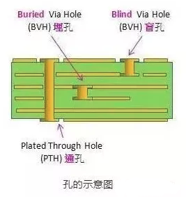
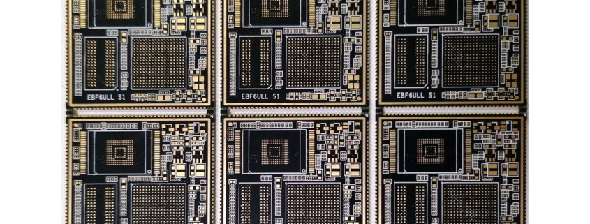
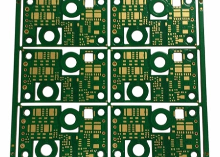
Conductive holes are also known as conductive holes. In order to meet customer requirements, circuit board via holes must be plugged. After a lot of practice, the traditional aluminum sheet plugging process was changed, and white mesh was used to complete the circuit board surface solder mask and plugging. hole. Stable production and reliable quality.
Via holes play the role of connecting circuits to each other. The development of the electronics industry also promotes the development of PCB and puts forward higher requirements for printed board manufacturing technology and surface mounting technology. Via hole plugging technology emerged as the times require, and it should meet the following requirements:
(1) There is only copper in the via hole, and the solder mask can be plugged or not;
(2) There must be tin-lead in the via hole, and there is a certain thickness requirement (4 microns). There must be no solder mask ink entering the hole, causing tin beads to be hidden in the hole;
(3) The via hole must be plugged with solder mask ink, opaque, and must not have tin rings, tin beads, and flatness.
As electronic products develop in the direction of “light, thin, short and small”, PCBs are also developing towards high density and difficulty. Therefore, a large number of SMT and BGA PCBs appear. Customers require plug holes when mounting components. The main ones are Five functions:
(1) Prevent tin from the via hole penetrating the component surface to cause a short circuit when the PCB is wave soldered; especially when we place the via hole on the BGA pad, we must first make a plug hole and then gold plating to facilitate the welding of the BGA.
(2) Avoid flux remaining in the via hole;
(3) After surface mounting and component assembly in the electronics factory are completed, the PCB must be vacuumed on the testing machine to form negative pressure before completion:
(4) Prevent surface solder paste from flowing into the holes, causing virtual soldering and affecting placement;
(5) Prevent tin beads from popping up during wave soldering and causing short circuits.
Implementation of conductive hole plugging process
For surface mount boards, especially the mounting of BGA and IC, the via holes must be flat, with a convexity of plus or minus 1 mil. There must be no red tinting on the edges of the via holes; tin beads are hidden in the via holes. In order to satisfy customers According to the requirements, the via hole plugging process can be described as diverse, the process flow is extremely long, and the process control is difficult. Problems such as oil leakage during hot air leveling and green oil solder resistance testing and oil explosion after curing often occur. Based on the actual production conditions, we will summarize various PCB hole plugging processes and make some comparisons and elaborations on the processes, advantages and disadvantages:
Note: The working principle of hot air leveling is to use hot air to remove excess solder from the surface and holes of the printed circuit board. The remaining solder is evenly covered on the pads, non-resisting solder lines and surface packaging points. It is a surface treatment method for printed circuit boards. one.
1. Hole plugging process after hot air leveling
This process flow is: board solder mask→HAL→hole plugging→curing. The non-hole plugging process is used for production. After hot air leveling, an aluminum sheet screen or an ink-blocking net is used to complete the via hole plugging of all fortresses required by the customer. The plugging ink can be photosensitive ink or thermosetting ink. Under the condition of ensuring that the color of the wet film is consistent, it is best to use the same ink as the board surface. This process can ensure that the via hole does not lose oil after hot air leveling, but it can easily cause the plug hole ink to contaminate the board surface and make it uneven. Customers can easily cause false soldering during mounting (especially in BGA). So many customers do not accept this method.
2. Hole plugging process before hot air leveling
2.1 Plug the holes with aluminum sheets, solidify, and grind the plate for pattern transfer.
In this process, a CNC drilling machine is used to drill out the aluminum sheet that needs to be plugged, and the holes are made into a screen to plug the holes to ensure that the via holes are filled with plugging ink. The plugging ink can also be thermosetting ink, which must have high hardness. , the resin shrinkage changes little, and the bonding force with the hole wall is good. The process flow is: pre-processing → hole plugging → plate grinding → pattern transfer → etching → solder mask on the board surface
This method can ensure that the via hole plug hole is flat, and hot air leveling will not cause quality problems such as oil explosion and oil loss on the edge of the hole. However, this process requires one-time thickening of copper to make the hole wall copper thickness meet the customer’s standards. Therefore, there are very high requirements for copper plating on the entire board, and there are also high requirements for the performance of the plate grinding machine to ensure that the resin on the copper surface is completely removed and the copper surface is clean and not contaminated. Many PCB factories do not have a one-time copper thickening process, and the performance of the equipment does not meet the requirements, resulting in this process being rarely used in PCB factories.
2.2 Plug the holes with aluminum sheets and directly screen-print the solder mask on the board.
In this process, a CNC drilling machine is used to drill out the aluminum sheet that needs to be plugged, and the screen is made into a screen. It is installed on the screen printing machine to plug the holes. After the plugging is completed, it should not be parked for more than 30 minutes. A 36T screen is used to directly screen the board surface to resist soldering. The process flow is: pre-treatment – hole plugging – screen printing – pre-baking – exposure – development – curing
Using this process can ensure that the via holes are well covered, the plug holes are flat, and the wet film has the same color. After hot air leveling, it can ensure that the via holes are not tinned and there are no tin beads hidden in the holes. However, it is easy to cause the ink in the holes to be stained after curing. pad, resulting in poor solderability; after hot air leveling, the edges of the via holes bubble and oil is removed. Production control using this process is difficult, and process engineers must adopt special processes and parameters to ensure the quality of the plug holes.
2.3 After the aluminum sheet is plugged, developed, pre-cured, and ground, the board surface is soldered.
Use a CNC drilling machine to drill out the aluminum sheet that requires plugging holes, make a screen, install it on a shift screen printing machine to plug the holes, the plug holes must be full, preferably protruding on both sides, and then solidify and grind the plate for surface treatment. The process flow is: pre-processing – hole plugging – pre-baking – development – pre-curing – solder mask on the board
Since this process uses plug hole curing, it can ensure that the via holes do not lose oil or explode after HAL. However, after HAL, it is difficult to completely solve the problem of tin beads hiding in via holes and tin application on via holes, so many customers do not accept it.
2.4 The solder mask and plug holes on the board are completed at the same time.
This method uses a 36T (43T) screen, installed on the screen printing machine, using a backing plate or nail bed to plug all the via holes while completing the board. The process flow is: pre-processing – screen printing – -Pre-baking–exposure–development–curing.
This process takes a short time and has a high utilization rate of the equipment. It can ensure that no oil will fall out of the via holes after hot air leveling, and no tin will be applied to the conductive holes. However, due to the use of silk screen printing for plugging, there is a large amount of air in the via holes, which will cause a large amount of air in the via holes during curing. , the air expands and breaks through the solder mask, causing holes and unevenness. Hot air leveling will leave a small amount of tin hidden in the via holes. At present, after a lot of experiments, our company has selected different types of inks and viscosities, adjusted the pressure of screen printing, etc., and basically solved the voids and unevenness of the vias, and has adopted this process for mass production.
https://bestpcb-ems.com/wp-content/uploads/2024/06/232.jpg397640administratorhttps://bestpcb-ems.com/wp-content/uploads/2023/05/logo-pcb2.pngadministrator2024-06-30 05:13:222024-06-30 05:13:26What is the science of plugging holes in PCB circuit boards?
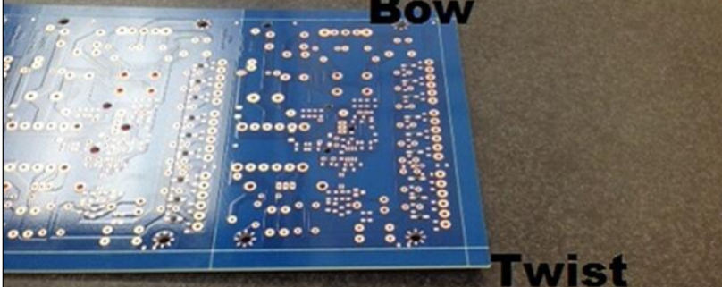
In automated surface mounting lines, if the circuit board is not flat, it will cause inaccurate positioning, components cannot be inserted or mounted into the board’s holes and surface mounting pads, and the automatic insertion machine may even be damaged.
The circuit board with the components on it is bent after soldering, and it is difficult to cut the component pins neatly. The board cannot be installed into the chassis or the socket inside the machine, so it is also very troublesome for the assembly factory to encounter a warped board.
The current surface mount technology is developing in the direction of high precision, high speed and intelligence, which puts forward higher flatness requirements for PCB boards, which are the homes of various components.
In the IPC standard, it is specifically stated that the allowable deformation of PCB boards with surface mount devices is 0.75%, and the allowable deformation of PCB boards without surface mount devices is 1.5%.
In fact, in order to meet the needs of high-precision and high-speed placement, some electronic assembly manufacturers have stricter requirements for deformation. If required, the allowed deformation is 0.5%, and some even require 0.3%.
PCB boards are composed of copper foil, resin, glass cloth and other materials. The physical and chemical properties of each material are different. After being pressed together, thermal stress residues will inevitably occur, leading to deformation.
At the same time, during the processing of PCB, various processes such as high temperature, mechanical cutting, and wet treatment will also have an important impact on the deformation of the board. In short, the causes of PCB board deformation are complex and diverse. How to reduce or eliminate the deformation due to material characteristics? Deformation caused by differences or processing has become one of the complex problems faced by PCB manufacturers.
Analysis of causes of PCB board deformation
The deformation of PCB board needs to be studied from several aspects such as material, structure, pattern distribution, processing process, etc. This article will analyze and elaborate on the various causes of possible deformation and improvement methods.
The uneven copper surface area on the circuit board will worsen the board bending and warping.
Generally, circuit boards are designed with a large area of copper foil for grounding purposes. Sometimes the Vcc layer is also designed with a large area of copper foil. When these large area copper foils cannot be evenly distributed on the same circuit board When it is installed, it will cause the problem of uneven heat absorption and heat dissipation speed.
Of course, the circuit board will also expand due to thermal expansion and contraction. If the expansion and contraction cannot occur at the same time, it will cause different stresses and deformation. At this time, if the temperature of the board has reached the upper limit of the Tg value, the board will begin to soften, causing deformation.
The connection points (vias, vias) of each layer on the circuit board will limit the expansion and contraction of the board.
Most of today’s circuit boards are multi-layer boards, and there are connection points (vias) like rivets between layers. The connection points are divided into through holes, blind holes and buried holes. Where there are connection points, the board will be restricted. The effect of expansion and contraction will also indirectly cause the board to bend and warp.
Reasons for PCB board deformation:
(1) The weight of the circuit board itself will cause the board to dent and deform.
Generally, reflow furnaces use chains to drive the circuit board forward in the reflow furnace, that is, using both sides of the board as fulcrums to support the entire board.
If there are overweight parts on the board, or the size of the board is too large, there will be a dent in the middle due to its own weight, causing the board to bend.
(2) The depth of the V-Cut and the connecting strip will affect the deformation of the panel.
Basically, V-Cut is the culprit that destroys the structure of the board. Because V-Cut cuts grooves into the original large sheet, the V-Cut is prone to deformation.
The influence of laminating materials, structures, and graphics on plate deformation:
The PCB board is composed of a core board, a prepreg, and an outer layer of copper foil. The core board and copper foil are thermally deformed during lamination. The amount of deformation depends on the coefficient of thermal expansion (CTE) of the two materials.
The thermal expansion coefficient (CTE) of copper foil is about 17X10-6; while the Z-direction CTE of ordinary FR-4 substrate at the Tg point is (50~70)X10-6; above the TG point it is (250~350)X10-6 , X-direction CTE is generally similar to copper foil due to the presence of glass cloth.
Deformation caused during PCB board processing
The causes of PCB board deformation during processing are very complex and can be divided into two types of stress: thermal stress and mechanical stress.
Thermal stress is mainly generated during the lamination process, and mechanical stress is mainly generated during the stacking, handling, and baking processes of panels. The following is a brief discussion in process order.
1. Incoming copper clad laminate materials:
Copper-clad laminates are all double-sided with symmetrical structure and no graphics. The CTE of copper foil and glass cloth are almost the same, so there is almost no deformation caused by different CTE during the lamination process.
However, the size of the copper-clad laminate press is large, and there are temperature differences in different areas of the hot plate, which will lead to slight differences in the resin curing speed and degree in different areas during the lamination process. At the same time, the dynamic viscosity at different heating rates is also significantly different, so there will also be Local stresses due to differences in the curing process.
Generally, this stress will maintain balance after pressing, but will gradually release and cause deformation during subsequent processing.
2. Pressing:
The PCB lamination process is the main process that generates thermal stress. Similar to the lamination of copper-clad laminates, it will also produce local stress caused by differences in the curing process. The thermal stress of PCB boards is due to thicker thickness, diverse pattern distribution, and more prepregs. The stress will also be more difficult to eliminate than that of copper clad laminate.
The stress existing in the PCB board is released during subsequent drilling, shaping or grilling processes, causing the board to deform.
3. Baking process of solder mask, characters, etc.:
Since the solder mask ink cannot be stacked on top of each other when curing, the PCB boards will be placed vertically in a rack for curing. The solder mask temperature is about 150°C, which is just above the Tg point of medium and low Tg materials. The resin above the Tg point is in a highly elastic state, and the board Parts are easily deformed under their own weight or strong wind from the oven.
4. Hot air solder leveling:
When leveling hot air solder for ordinary boards, the tin furnace temperature is 225℃~265℃ and the time is 3S-6S. The hot air temperature is 280℃~300℃.
The solder leveling plate enters the tin furnace at room temperature, and is post-processed and washed at room temperature within two minutes after coming out of the furnace. The entire hot air solder leveling process is a sudden heating and cooling process.
Due to different circuit board materials and uneven structures, thermal stress will inevitably occur during the cooling and heating process, resulting in microscopic strain and overall deformation and warping.
5. Storage:
PCB boards are generally stored vertically in racks during the semi-finished product stage. Improper adjustment of the rack’s tightness or stacking of boards during storage will cause mechanical deformation of the boards. Especially for thin plates below 2.0mm, the impact is more serious.
In addition to the above factors, there are many factors that affect PCB board deformation.
Prevention of PCB board warpage and deformation
Circuit board warpage has a great impact on the production of printed circuit boards. Warpage is also one of the important problems in the circuit board production process. The board with components on it will bend after welding, making it difficult for the component legs to be neat.
The board cannot be installed into the chassis or the socket inside the machine. Therefore, the warping of the circuit board will affect the normal operation of the entire subsequent process.
At this stage, printed circuit boards have entered the era of surface mounting and chip mounting, and the process requirements for circuit board warpage are getting higher and higher. So we need to find the reason why the circuit board is warping.
1. Engineering design:
Things to note when designing printed circuit boards:
A. The arrangement of prepreg sheets between layers should be symmetrical. For example, for a six-layer board, the thickness between layers 1 to 2 and 5 to 6 should be consistent with the number of prepreg sheets, otherwise it will easily warp after lamination.
B. Multilayer core boards and prepregs should use products from the same supplier.
C. The line pattern areas on the outer layer A and B should be as close as possible. If side A is a large copper surface and side B only has a few lines, this kind of printed board will easily warp after etching. If the line areas on the two sides are too different, you can add some independent grids on the sparse side for balance.
2. Drying plate before unloading:
The purpose of drying the copper-clad laminate (150 degrees Celsius, 8 ± 2 hours) before unloading is to remove the moisture in the board, and at the same time completely solidify the resin in the board, further eliminating the remaining stress in the board, which is helpful in preventing the board from warping. helpful.
At present, many double-sided and multi-layer boards still adhere to the step of drying the boards before or after cutting. However, there are exceptions for some board factories. Currently, the drying time regulations of various PCB factories are inconsistent, ranging from 4 to 10 hours. It is recommended to decide based on the grade of the printed boards produced and the customer’s requirements for warpage.
Both methods are feasible, whether to cut the pieces into panels and then bake them or to bake them as a whole piece and cut them out. It is recommended to cut the materials and then bake them. The inner layer boards should also be baked.
3. Longitude and latitude direction of prepreg:
The warp and weft shrinkage rates of prepregs after lamination are different, and the warp and weft directions must be distinguished when blanking and laminating. Otherwise, it is easy to cause the finished board to warp after lamination, which is difficult to correct even if pressure is applied to bake the board.
Many reasons for the warping of multi-layer boards are caused by not distinguishing the longitude and weft directions of the prepreg sheets during lamination, and they are stacked randomly.
How to distinguish longitude and latitude? The rolling direction of the rolled prepreg is the warp direction, and the width direction is the weft direction; for copper foil boards, the long side is the weft direction, and the short side is the warp direction. If you are not sure, you can check with the manufacturer or supplier.
4. Stress relief after lamination:
After completing the hot and cold pressing, the multi-layer board is taken out, the burrs are cut or milled, and then placed flat in an oven at 150 degrees Celsius for 4 hours to gradually release the stress in the board and completely solidify the resin. This step cannot be omitted.
5. Thin sheets need to be straightened during electroplating:
When using 0.4~0.6mm ultra-thin multi-layer boards for surface electroplating and pattern electroplating, special clamp rollers should be made. After clamping the thin plate on the fly bar of the automatic electroplating line, use a round stick to clamp the entire fly bar. The rollers are strung together to straighten all the boards on the rollers so that the plated boards will not deform.
Without this measure, the sheet will bend after plating a copper layer of 20 to 30 microns, and it will be difficult to repair.
6. Cooling of the board after hot air leveling:
During hot air leveling, the printed board is subjected to the high temperature impact of the soldering bath (about 250 degrees Celsius). After being taken out, it should be placed on a flat marble or steel plate to cool naturally, and then sent to the post-processing machine for cleaning. This is very good for preventing the board from warping.
In order to enhance the brightness of the lead-tin surface, some factories put the board into cold water immediately after being leveled with hot air, and then take it out after a few seconds for post-processing. This kind of hot and cold impact may cause warping of some types of boards. Curved, layered or blistered.
In addition, an air flotation bed can be installed on the equipment for cooling.
7. Treatment of warped boards:
In a well-managed factory, 100% flatness inspection of printed boards will be carried out during final inspection. All unqualified boards will be picked out, placed in an oven, baked at 150 degrees Celsius under heavy pressure for 3 to 6 hours, and allowed to cool naturally under heavy pressure.
Then remove the pressure and take out the board, and then check the flatness. This can save part of the board. Some boards need to be baked and pressed two to three times before they can be flattened. If the above-mentioned anti-warping process measures are not implemented, baking and pressing some boards will be useless and they will have to be scrapped.
https://bestpcb-ems.com/wp-content/uploads/2024/06/231.png368808administratorhttps://bestpcb-ems.com/wp-content/uploads/2023/05/logo-pcb2.pngadministrator2024-06-30 05:10:142024-06-30 05:10:14Why does the PCB board warp? Why does it cause so much harm after deformation?
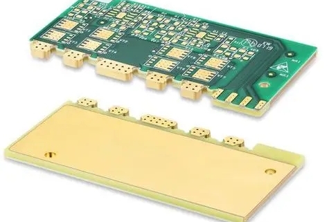
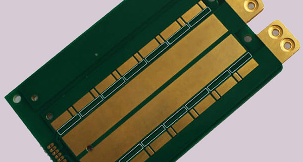
Circuit boards play a vital role in electronic equipment, and the customization of their thick copper plates is crucial to the stability and reliability of the equipment. This article will discuss in detail the customization of thick copper plates for circuit boards from four aspects: the advantages, customization process, application scenarios and future development trends of thick copper plates.
1. Advantages
As a special form of circuit board, thick copper plate has excellent thermal conductivity, good electrical performance and high strength, which plays a significant role in improving the stability and reliability of circuit boards. The thick copper plate can not only reduce the temperature rise of the circuit board and improve the heat dissipation performance, but also reduce the line loss of the circuit board and improve the accuracy of signal transmission. In special application areas such as high frequency and high power, thick copper plates are an indispensable choice. The advantage of thick copper plates is that they can provide better current carrying capacity, reduce the parasitic resistance of the circuit board, reduce the temperature of the circuit board, and extend the service life of the equipment. Therefore, customizing thick copper circuit boards can improve the reliability and stability of electronic equipment and is favored by more and more customers.
2. Customization process
The customization of thick copper plates for circuit boards usually requires the following processes: design confirmation, process discussion, material selection, production and processing, quality inspection and other links. The design confirmation stage is to determine customer needs and specifications. The process discussion stage includes determining the production process and requirements. The material selection stage is to select suitable copper and aluminum-based materials. The production and processing stage is to make circuit boards according to the design requirements. The quality inspection stage is to inspect the finished product. Conduct strict testing to ensure reliable quality. Due to the high production requirements for thick copper sheets for circuit boards, customers need to work closely with suppliers to ensure that every step of the process meets the requirements, so as to obtain customized products with reliable quality.
3. Application scenarios
Circuit board thick copper plates are widely used in communication equipment, military equipment, medical equipment, aerospace and other fields. In communication equipment, thick copper plates can increase signal transmission rate, reduce signal distortion rate, and ensure stable operation of equipment; in military equipment, thick copper plates have strong anti-interference and earthquake resistance, and can adapt to various harsh environments; in medical equipment Medium and thick copper plates can improve the safety and stability of equipment and ensure the accuracy of medical operations; in the aerospace field, thick copper plates can meet the requirements for lightweight and high performance of equipment and ensure long-term stable operation of equipment.
4. Future development trends
As the requirements for stability and reliability of electronic equipment continue to increase, the market demand for thick copper sheets for circuit boards will continue to grow. In the future, customized thick copper plates will pay more attention to the selection of environmentally friendly materials and develop more energy-saving and environmentally friendly thick copper plates for circuit boards; at the same time, with the development of technologies such as intelligence and the Internet of Things, thick copper plates for circuit boards will play an important role in the development of new smart devices. It has an important impact on applications and becomes an indispensable key component in future electronic devices.
The customization of thick copper plates for circuit boards is the best choice to improve the stability and reliability of electronic equipment, which is of great significance and broad prospects. By continuously optimizing the process flow and expanding the application fields, circuit board thick copper plates will be more widely used in various types of electronic equipment in the future, injecting more vitality into the development of the electronics industry.
https://bestpcb-ems.com/wp-content/uploads/2024/06/229.jpg10001000administratorhttps://bestpcb-ems.com/wp-content/uploads/2023/05/logo-pcb2.pngadministrator2024-06-30 05:04:372024-06-30 05:04:55Customized thick copper circuit board, the best choice for stability and reliability!
1. Overview of sensor pcb board
The sensor PCB board is a circuit board specially used for sensors, mainly used to measure and detect changes in environmental conditions or object characteristics. It realizes signal collection, processing and transmission by combining sensor elements with circuit boards. Among them, common sensor PCBs mainly include temperature sensor PCBs, photoelectric sensor PCBs, pressure sensor PCBs, etc.
2. Temperature sensor pcb
Temperature sensor PCB is mainly used to measure and control the temperature of objects. The sensor elements used are usually thermistors, thermocouples or semiconductor temperature sensors. By tightly integrating sensor components with PCB, real-time monitoring and control of temperature can be achieved, which is widely used in home appliances, automobiles, medical equipment and other fields.
3. Photoelectric sensor PCB
Photoelectric sensor PCB is mainly used to detect the light intensity and position of objects. Common photoelectric sensor PCB types include photoresistor sensor PCB, photodiode sensor PCB, laser sensor PCB, etc. By combining these sensor components with PCB, functions such as measurement of light intensity and position detection of objects can be realized, and are widely used in fields such as automation control and security monitoring.
4. Pressure sensor pcb
Pressure sensor pcb is used to measure pressure changes of gas or liquid. The sensor elements usually use piezoresistive, capacitive or electronic oscillator sensors. By combining these sensor components with PCBs, pressure monitoring and control can be achieved, and are widely used in industrial automation, energy management, environmental monitoring and other fields.
Sensor PCBs play an important role in various fields. By combining with different types of sensor elements, they can achieve accurate measurement and control of physical quantities such as temperature, light intensity, and pressure. With the continuous advancement of technology, sensor PCBs will be more widely used in various industries, bringing more convenience and innovation to our lives and work.
https://bestpcb-ems.com/wp-content/uploads/2024/06/228.jpg836834administratorhttps://bestpcb-ems.com/wp-content/uploads/2023/05/logo-pcb2.pngadministrator2024-06-30 05:03:042024-06-30 05:03:11What are the PCB sensors? Sensor PCB board revealed!
In recent years, with the rapid development of science and technology, the application scope of PCB (Printed Circuit Board) thick copper plates has gradually expanded, and it has shown an amazing multi-faceted identity in various fields. This article will focus on the PCB thick copper plate and explore its wide range of applications in the electronic field.
1. Power electronics applications
PCB thick copper plate plays a vital role in the field of power electronics. In high-power equipment such as power amplifiers, inverters, and rectifiers, the use of PCB thick copper plates can effectively improve heat dissipation performance and ensure stable operation of the equipment under high loads. Due to its excellent heat dissipation characteristics, PCB thick copper plates are widely used in various industrial power supplies, UPS, transformers and other equipment. In power electronic equipment, PCB thick copper plates can not only provide good heat dissipation effects, but also increase current carrying capacity, reduce resistance and losses, and improve equipment performance and reliability. Therefore, PCB thick copper plate has become one of the indispensable key materials in the power electronics industry.
2. Automotive electronics field
With the rapid development of automotive electronics technology, PCB thick copper plates have also shown strong application potential in the field of automotive electronics. In fields such as electric vehicles, smart driving, and in-vehicle entertainment systems, PCB thick copper plates can provide stable and reliable electrical connections to meet the needs of high-power and high-frequency electronic equipment. In addition, automotive electronic equipment often needs to work in harsh working environments, such as high temperature, high humidity, vibration and other conditions. The high strength, high reliability and stable performance of PCB thick copper plate make it an ideal choice in the automotive electronics industry.
3. Communication equipment applications
In the field of communication equipment, such as base stations, satellite communications, wireless networks and other equipment, PCB thick copper plates also play a key role. Since communication equipment needs to carry high-power, high-frequency signals, the low resistance, high thermal conductivity and stable performance of PCB thick copper plates make them popular in this field. PCB thick copper plates can not only improve the stability and speed of signal transmission in communication equipment, but also reduce the size of the circuit board and improve the integration and performance of the equipment. Therefore, communication equipment manufacturers are increasingly inclined to use PCB thick copper plates to meet the demand for high-power, high-frequency equipment.
4. Aerospace applications
In the aerospace field, the requirements for electronic equipment are more stringent, and the application of PCB thick copper plates is also more prominent. Aerospace equipment needs to have the characteristics of lightweight, high reliability and high temperature resistance, and PCB thick copper plate can meet these needs. PCB thick copper plates can withstand the working environment under harsh conditions such as high temperature, high pressure and strong vibration in aerospace equipment, ensuring the normal operation of electronic equipment. At the same time, PCB thick copper plates can also meet the needs of aerospace equipment for high-power and high-frequency electronic devices, ensuring equipment performance and safety.
PCB thick copper plates are widely used in power electronics, automotive electronics, communication equipment, aerospace and other fields. Its excellent heat dissipation performance, high current carrying capacity and stable performance make it an indispensable and key component in the modern electronics industry. With the continuous advancement of technology and the expansion of application fields, PCB thick copper plates will continue to play an important role in promoting the development and innovation of electronic equipment.
https://bestpcb-ems.com/wp-content/uploads/2024/06/223.webp.jpg500667administratorhttps://bestpcb-ems.com/wp-content/uploads/2023/05/logo-pcb2.pngadministrator2024-06-30 04:55:372024-06-30 04:55:42What fields are thick copper PCB used in? Unlock the multi-faceted identity of thick copper PCB!
Circuit board thick copper board is an indispensable key component in electronic equipment. It provides stable electrical connection and good thermal conductivity, providing strong power for the normal operation of the equipment. This article will elaborate on the thick copper board of circuit board from the following four aspects, including material properties, manufacturing process, application fields and future development trends.
1. Material properties
Thick copper boards have excellent electrical conductivity and thermal conductivity. Compared with ordinary circuit boards, thick copper boards have higher current carrying capacity and lower line impedance, and can meet the needs of high-frequency and high-power equipment. In addition, thick copper plates also have good corrosion resistance and mechanical strength, and can operate stably in various harsh environments.
2. Manufacturing process
The manufacturing process of thick copper boards is relatively complex and requires multiple processes. The first is material selection and cutting. Select copper plates with high purity and fine crystallization as raw materials, and use precision cutting equipment to cut them into the required shape. Then comes surface treatment, including chemical cleaning and anti-oxidation treatment to ensure the purity and stability of the circuit board surface. Next comes pattern drawing and copper lamination, using photolithography technology for image transfer, and laminating the copper foil to the substrate through high temperature and high pressure. Finally, there are processes such as drilling, lead-tin plating, printing and testing to complete the manufacturing of the entire circuit board.
3. Application fields
Thick copper boards are widely used in various high-power and high-frequency electronic equipment, including communication equipment, computer equipment, power supply equipment, automotive electronics, etc. In communication equipment, thick copper plates are used to make high-frequency radio frequency modules and antennas; in computer equipment, thick copper plates are used to make high-performance CPU radiators and cooling modules; in power supply equipment, thick copper plates are used to make high-performance Current DC bus and current sampling resistor, etc. Due to its excellent performance, thick copper boards are also widely used in fields such as new energy vehicles and aerospace.
4. Future development trends
With the continuous development and upgrading of electronic equipment, the requirements for circuit boards are becoming higher and higher. In the future, circuit board thick copper boards will continue to develop towards high density, high performance and multi-function. For example, multi-layer stacking technology and new materials are used to achieve a more compact design and higher circuit integration; advanced heat dissipation technology is used to improve heat dissipation efficiency and meet the thermal management needs of new generation equipment; flexible circuit technology is used to achieve Bending and folding expand the application scenarios of circuit boards. To sum up, circuit board thick copper plate is the key to success in electronic equipment and will help technology achieve new breakthroughs in continuous innovation and development.
As a key component in electronic equipment, circuit board thick copper boards have excellent material properties and manufacturing processes. It is widely used in many fields and provides strong power for the normal operation of equipment. With the continuous development and advancement of electronic equipment, thick copper boards will continue to develop in terms of high density, high performance and multi-function, helping to achieve technological breakthroughs. It is believed that circuit board thick copper board manufacturers will continue to provide innovative products and services to meet market demand and promote the development of the electronics industry.
https://bestpcb-ems.com/wp-content/uploads/2024/06/118.webp.jpg475475administratorhttps://bestpcb-ems.com/wp-content/uploads/2023/05/logo-pcb2.pngadministrator2024-06-30 04:37:582024-06-30 04:38:06Strong power is the key to victory! Circuit board thick copper board manufacturer helps you achieve technological breakthroughs!
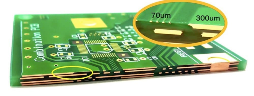
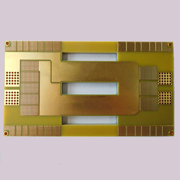
PCB half-hole boards are widely used in practical applications, but there are also some attention requirements in their processing. This article explains these issues in detail, including the design, processing and testing of half-hole boards, to help readers more clearly understand the adverse consequences during the processing process.
1. Design principles of half-hole board
Issues that need to be paid attention to when designing half-hole boards include plate thickness, board edge conditions, opening matching and scratches, etc. This article explains these issues one by one to ensure the rationality and stability of the half-hole plate design.
2. Things to note when processing half-hole boards
Half-hole boards processing involves drilling, milling, welding and other links. When drilling, you need to pay attention to aperture, plate slack, drill core offset and other issues; when milling slots, you need to pay attention to route planning, cutting allowance and other issues; when welding, you need to master skills such as pad size, ringing and welding slag.
3. Methods and standards for half-well board testing
After half-hole board processing is completed, strict testing is required to ensure its quality and stability. Commonly used inspection methods include visual inspection, high-power microscope inspection, sheet metal machine inspection, etc.; commonly used standards include IPC-6012, MIL-P-50884, etc.
4. Storage and transportation of half-well boards
Half-well boards are susceptible to mechanical damage, moisture oxygen corrosion, etc. during storage and transportation. This article provides an in-depth analysis of these issues and provides some effective storage and transportation tips to avoid undesirable half-well plates during transportation.
PCB half-hole boards design and processing requires some necessary skills and experience, and its inspection and storage also require attention to some specific details. Only by completing these details can the half-hole board have high stability and reliability in practical applications.
https://bestpcb-ems.com/wp-content/uploads/2024/06/88.jpg10001361administratorhttps://bestpcb-ems.com/wp-content/uploads/2023/05/logo-pcb2.pngadministrator2024-06-17 08:57:152024-06-17 08:57:19Are there any requirements for attention during the processing of half-hole pcb?
Circuit board thick copper board is an indispensable key component in electronic equipment. It provides stable electrical connection and good thermal conductivity, providing strong power for the normal operation of the equipment. This article will elaborate on the thick copper board of circuit board from the following four aspects, including material properties, manufacturing process, application fields and future development trends.
1. Material properties
Thick copper boards have excellent electrical conductivity and thermal conductivity. Compared with ordinary circuit boards, thick copper boards have higher current carrying capacity and lower line impedance, and can meet the needs of high-frequency and high-power equipment. In addition, thick copper plates also have good corrosion resistance and mechanical strength, and can operate stably in various harsh environments.
2. Manufacturing process
The manufacturing process of thick copper boards is relatively complex and requires multiple processes. The first is material selection and cutting. Select copper plates with high purity and fine crystallization as raw materials, and use precision cutting equipment to cut them into the required shape. Then comes surface treatment, including chemical cleaning and anti-oxidation treatment to ensure the purity and stability of the circuit board surface. Next comes pattern drawing and copper lamination, using photolithography technology for image transfer, and laminating the copper foil to the substrate through high temperature and high pressure. Finally, there are processes such as drilling, lead-tin plating, printing and testing to complete the manufacturing of the entire circuit board.
3. Application fields
Thick copper boards are widely used in various high-power and high-frequency electronic equipment, including communication equipment, computer equipment, power supply equipment, automotive electronics, etc. In communication equipment, thick copper plates are used to make high-frequency radio frequency modules and antennas; in computer equipment, thick copper plates are used to make high-performance CPU radiators and cooling modules; in power supply equipment, thick copper plates are used to make high-performance Current DC bus and current sampling resistor, etc. Due to its excellent performance, thick copper boards are also widely used in fields such as new energy vehicles and aerospace.
4. Future development trends
With the continuous development and upgrading of electronic equipment, the requirements for circuit boards are becoming higher and higher. In the future, circuit board thick copper boards will continue to develop towards high density, high performance and multi-function. For example, multi-layer stacking technology and new materials are used to achieve a more compact design and higher circuit integration; advanced heat dissipation technology is used to improve heat dissipation efficiency and meet the thermal management needs of new generation equipment; flexible circuit technology is used to achieve Bending and folding expand the application scenarios of circuit boards. To sum up, circuit board thick copper plate is the key to success in electronic equipment and will help technology achieve new breakthroughs in continuous innovation and development.
As a key component in electronic equipment, circuit board thick copper boards have excellent material properties and manufacturing processes. It is widely used in many fields and provides strong power for the normal operation of equipment. With the continuous development and advancement of electronic equipment, thick copper boards will continue to develop in terms of high density, high performance and multi-function, helping to achieve technological breakthroughs. It is believed that circuit board thick copper board manufacturers will continue to provide innovative products and services to meet market demand and promote the development of the electronics industry.
https://bestpcb-ems.com/wp-content/uploads/2024/06/80.jpg450450administratorhttps://bestpcb-ems.com/wp-content/uploads/2023/05/logo-pcb2.pngadministrator2024-06-17 08:50:072024-06-17 08:50:11Strong power is the key to victory! Circuit board thick copper board manufacturer helps you achieve technological breakthroughs!
In recent years, with the rapid development of science and technology, the application scope of PCB (Printed Circuit Board) thick copper plates has gradually expanded, and it has shown an amazing multi-faceted identity in various fields. This article will focus on the PCB thick copper plate and explore its wide range of applications in the electronic field.
1. Power electronics applications
PCB thick copper plate plays a vital role in the field of power electronics. In high-power equipment such as power amplifiers, inverters, and rectifiers, the use of PCB thick copper plates can effectively improve heat dissipation performance and ensure stable operation of the equipment under high loads. Due to its excellent heat dissipation characteristics, PCB thick copper plates are widely used in various industrial power supplies, UPS, transformers and other equipment. In power electronic equipment, PCB thick copper plates can not only provide good heat dissipation effects, but also increase current carrying capacity, reduce resistance and losses, and improve equipment performance and reliability. Therefore, PCB thick copper plate has become one of the indispensable key materials in the power electronics industry.
2. Automotive electronics field
With the rapid development of automotive electronics technology, PCB thick copper plates have also shown strong application potential in the field of automotive electronics. In fields such as electric vehicles, smart driving, and in-vehicle entertainment systems, PCB thick copper plates can provide stable and reliable electrical connections to meet the needs of high-power and high-frequency electronic equipment. In addition, automotive electronic equipment often needs to work in harsh working environments, such as high temperature, high humidity, vibration and other conditions. The high strength, high reliability and stable performance of PCB thick copper plate make it an ideal choice in the automotive electronics industry.
3. Communication equipment applications
In the field of communication equipment, such as base stations, satellite communications, wireless networks and other equipment, PCB thick copper plates also play a key role. Since communication equipment needs to carry high-power, high-frequency signals, the low resistance, high thermal conductivity and stable performance of PCB thick copper plates make them popular in this field. PCB thick copper plates can not only improve the stability and speed of signal transmission in communication equipment, but also reduce the size of the circuit board and improve the integration and performance of the equipment. Therefore, communication equipment manufacturers are increasingly inclined to use PCB thick copper plates to meet the demand for high-power, high-frequency equipment.
4. Aerospace applications
In the aerospace field, the requirements for electronic equipment are more stringent, and the application of PCB thick copper plates is also more prominent. Aerospace equipment needs to have the characteristics of lightweight, high reliability and high temperature resistance, and PCB thick copper plate can meet these needs. PCB thick copper plates can withstand the working environment under harsh conditions such as high temperature, high pressure and strong vibration in aerospace equipment, ensuring the normal operation of electronic equipment. At the same time, PCB thick copper plates can also meet the needs of aerospace equipment for high-power and high-frequency electronic devices, ensuring equipment performance and safety.
PCB thick copper plates are widely used in power electronics, automotive electronics, communication equipment, aerospace and other fields. Its excellent heat dissipation performance, high current carrying capacity and stable performance make it an indispensable and key component in the modern electronics industry. With the continuous advancement of technology and the expansion of application fields, PCB thick copper plates will continue to play an important role in promoting the development and innovation of electronic equipment.
https://bestpcb-ems.com/wp-content/uploads/2024/06/79.jpg600600administratorhttps://bestpcb-ems.com/wp-content/uploads/2023/05/logo-pcb2.pngadministrator2024-06-17 08:47:252024-06-17 08:47:30What fields are thick copper PCB used in? Unlock the multi-faceted identity of thick copper PCB!
 plications of fpc? First of all, FPC is widely used in mobile devices, such as smartphones, tablets, etc. Because FPC has high flexibility and foldability, it can adapt to the needs of equipment of various shapes and sizes. Secondly, it is also widely used in the field of automotive electronics. In cars, FPC can connect various sensors, displays and control modules to realize vehicle intelligence and automation. In addition, it is also commonly used in medical equipment, aerospace, industrial control and other fields to provide reliable circuit connections for various electronic devices.