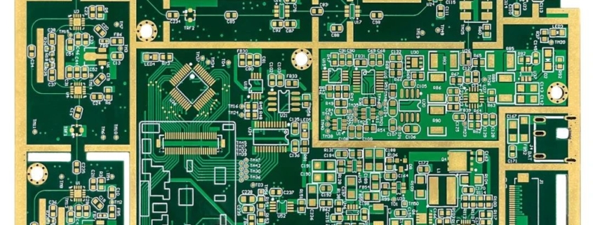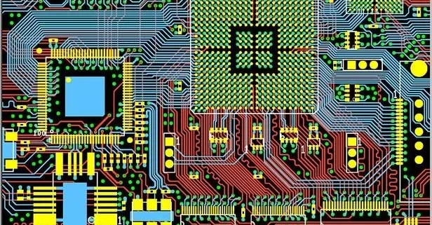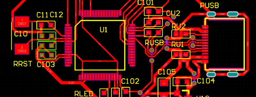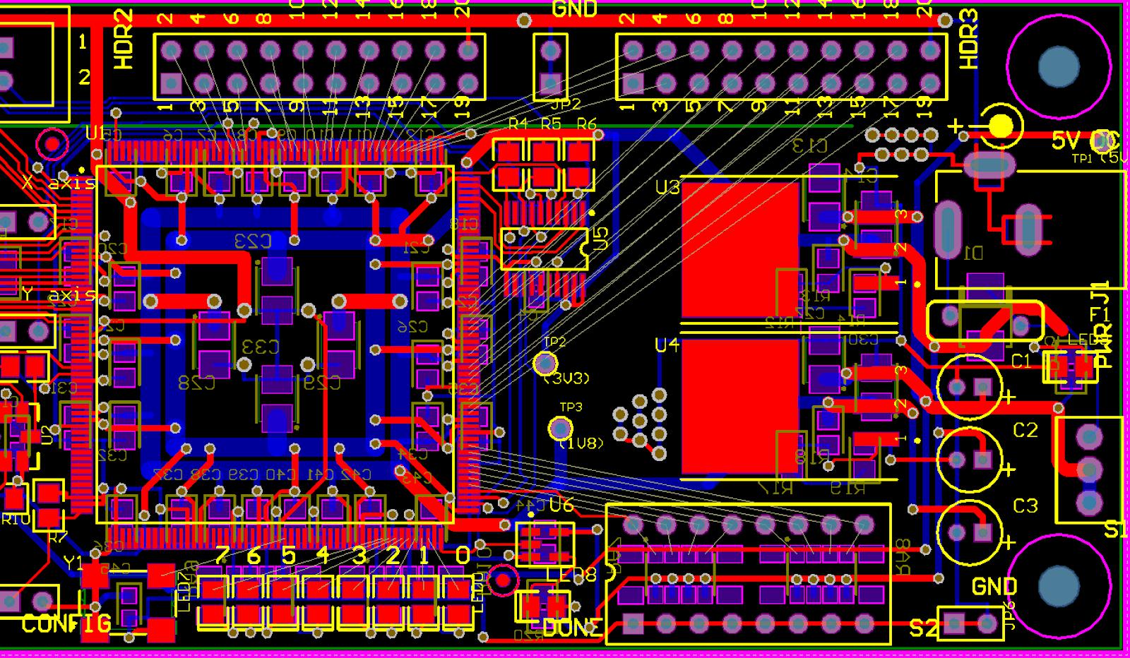
What are the PCB design requirements?
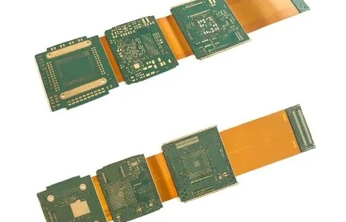
Today’s PCB technology mainly changes according to the characteristics and requirements of electronic products. In recent years, electronic products have become increasingly multi-functional, sophisticated and comply with environmental regulations. Therefore, the precision of PCB is getting higher and higher, and its application of combining soft and hard boards will also increase.
PCB is the foundation of the information industry. From computers to portable electronic devices, circuit boards are found in almost all electronic and electrical products. With the development of communication technology, handheld wireless radio frequency circuit technology is used more and more widely. One of the biggest characteristics of these devices (such as mobile phones, wireless PDAs, etc.) is: first, they include almost all portable subsystems; second, they are small Miniaturization means that the density of components is very high, which makes the mutual interference of components (including SMD, SMC, bare chips, etc.) very prominent. Therefore, it has become a very important topic to design a perfect PCB for RF circuits and audio circuits to prevent and suppress electromagnetic interference and thereby improve electromagnetic compatibility.
Because the performance indicators of the same circuit and different PCB design structures will vary greatly. Especially as the audio functions of today’s handheld products continue to increase, more attention must be paid to the PCB layout of the audio circuit. Based on this, this article focuses on the ingenious design of the PCB of the RF circuit and audio circuit of the handheld product (that is, including component layout, component arrangement, wiring and Grounding and other techniques) for analysis and explanation.
1. Component layout
First, let’s talk about the general principles of layout: components should be arranged in the same direction as much as possible, and the phenomenon of poor welding can be reduced or even avoided by choosing the direction in which the PCB enters the tin melting system; as known from practice, there must be at least 0.5mm spacing between components to meet the requirements of the components. Regarding the soldering requirements of the device, if the space of the PCB board allows, the spacing between components should be as wide as possible. For double-sided panels, one side should generally be designed with SMD and SMC components, and the other side should be designed with discrete components.
1.1 Divide the PCB into digital areas and analog areas.
The first step in any PCB design is, of course, choosing the PCB placement of each component. We call this step “layout consideration”. Careful component placement can reduce signal interconnections, ground separation, noise coupling, and occupied circuit board area.
Electromagnetic compatibility requires that each circuit module PCB is designed to produce as little electromagnetic radiation as possible and to have a certain anti-electromagnetic interference capability. Therefore, the layout of components also directly affects the interference and anti-interference capabilities of the circuit itself, which is also directly related to performance of the designed circuit.
Therefore, when designing an RF circuit PCB, in addition to considering the layout of ordinary PCB designs, you must also consider how to reduce the mutual interference between various parts of the RF circuit, how to reduce the interference of the circuit itself to other circuits, and the circuit itself. anti-interference ability.
It is known from experience that the quality of the RF circuit effect not only depends on the performance indicators of the RF circuit board itself, but also largely depends on the interaction with the CPU processing board. Since RF circuits contain digital circuits and analog circuits, in order to prevent digital noise from interfering with sensitive analog circuits, they must be separated. Dividing the PCB into digital areas and analog areas can help improve the layout of such circuits, which is particularly important. important.
1.2 Need to prevent RF noise from coupling into audio circuits
Although the RF portion of handheld products is often treated as analog circuitry, a common concern in many designs is RF noise. It is necessary to prevent RF noise from coupling into the audio circuitry, because the RF noise is demodulated to produce audible noise. In order to solve this problem, the RF circuit and the audio circuit need to be separated as much as possible. After dividing the PCB into analog and digital, the component layout of the analog part needs to be considered. The component layout should make the path of the audio signal the shortest, and the audio amplifier should be placed as close as possible to the headphone jack and speaker to minimize the EMI radiation of the Class D audio amplifier and the coupling noise of the headphone signal. The analog audio signal source must be as close as possible to the input of the audio amplifier to minimize input coupling noise. All input leads act as an antenna for RF signals, and shortening the lead length helps reduce the antenna radiation effect in the corresponding frequency band.
2. Issues that should be paid attention to in component layout and application examples
2.1 Issues that should be paid attention to in layout:
Carefully analyze the circuit structure. Divide circuits into blocks (such as high-frequency amplification circuits, mixing circuits and demodulation circuits, etc.) to separate strong current signals and weak current signals as much as possible. After separating digital signal circuits and analog signal circuits, attention should also be paid to Circuits that perform the same function should be arranged within a certain range as much as possible to reduce the signal loop area; the filter network of each part of the circuit must be connected nearby, which can not only reduce radiation, but also reduce the chance of interference and improve the efficiency of the circuit. anti-interference ability.
Unit circuits are grouped according to their different sensitivity to electromagnetic compatibility during use. For components in the circuit that are susceptible to interference, the layout should also try to avoid interference sources (such as interference from the CPU on the data processing board, etc.).
2.2 Examples of the impact of component placement on audio signals
The impact of unreasonable component layout on audio signal quality
An unreasonable layout of audio components has two serious problems: one is that the audio amplifier is too far away from the audio signal source, because the leads pass near noisy digital circuits and switching circuits, thereby increasing the probability of noise coupling. Longer leads also enhance the RF antenna effect. If a mobile phone uses GSM technology, these antennas can pick up the GSM transmitted signal and feed it into the audio amplifier. Almost all amplifiers can demodulate the 217Hz envelope to some extent, producing noise at the output. In the worst case, the noise may completely drown out the audio signal. Shortening the length of the input lead can effectively reduce the noise coupled to the audio amplifier. The second audio amplifier is placed too far away from the speaker and headphone jack.
If the audio amplifier uses a Class D amplifier, longer headphone leads will increase the EMI radiation of the amplifier. This radiation may cause the device to fail testing standards set by local governments. Longer headphone and microphone leads also increase lead impedance, reducing the power the load can draw. Finally, because the components are so spread out, the wires between them will have to pass through other subsystems. This will not only increase the wiring difficulty of the audio part, but also increase the wiring difficulty of other subsystems.
The impact of unreasonable component layout on audio signal quality
Reasonable component layout improves audio signal quality
Arrangement of the same components, rearranged components can use space more efficiently and shorten lead lengths. Note that all audio circuits are distributed near the headphone jack and speakers, the audio input and output leads are much shorter than the above solution, and no audio circuits are placed in other areas of the PCB. This design can comprehensively reduce system noise, reduce RF interference, and simplify wiring.
Reasonable component layout indicates the improvement of audio signal quality
3. Wiring principles and techniques
After the layout of the components is basically completed, wiring can begin.
3.1 Basic principles of wiring
When the assembly density permits, try to use a low-density wiring design, and keep the signal traces as consistent in thickness as possible to facilitate impedance matching.
For RF circuits, unreasonable design of the direction, width, and line spacing of signal lines may cause cross-interference between signal transmission lines. The signal path has a very limited impact on audio output noise and distortion, which means there are very few compromises that need to be made to ensure performance. Audio amplifiers are usually powered directly from batteries and require considerable current. If you use long, thin power supply leads, the power supply ripple will be increased. Compared with short and wide leads, long and thin leads have greater impedance, and the current changes generated by the lead impedance are converted into voltage changes and fed into the device. To optimize performance, amplifier power supplies should use the shortest possible leads. Differential signaling should be used whenever possible. Differential inputs have higher noise rejection, allowing the differential receiver to reject common-mode noise on both the positive and negative signal lines. To take full advantage of a differential amplifier, it is important to keep the differential signal pairs the same length when routing them, so that they have the same impedance, and that they are as close to each other as possible so that they couple the same amount of noise. The amplifier’s differential inputs are very effective at rejecting noise from the system’s digital circuitry. In addition, the system power supply itself also has noise interference, so comprehensive considerations must be taken when designing the RF circuit PCB and the wiring must be reasonable.
3.2 Wiring skills
When wiring, all traces should be kept away from the frame of the PCB board (about 2mm) to avoid wire breakage or potential risk of wire breakage during PCB board production. The power lines should be as wide as possible to reduce loop resistance. At the same time, the direction of the power lines and ground wires should be consistent with the direction of data transmission to improve anti-interference capabilities. The signal lines should be as short as possible and minimize excessive interference. The number of holes; the shorter the connections between components, the better, in order to reduce distribution parameters and mutual electromagnetic interference; incompatible signal lines should be kept away from each other, and try to avoid parallel wiring, and on both sides of the forward direction The signal lines should be perpendicular to each other; when wiring, the angle of 135° should be used at addresses that require corners, and avoid turning at right angles.
4. Grounding
In the design of RF circuit PCB, the correct wiring of power lines and ground wires is particularly important. Reasonable design is the most important means to overcome electromagnetic interference. A considerable number of interference sources on PCB are generated through power and ground wires, among which the ground wire causes the largest noise interference. The main reason why ground wires easily cause electromagnetic interference is that there is impedance in the ground wire. When a current flows through the ground wire, a voltage will be generated on the ground wire, resulting in a ground loop current and causing loop interference in the ground wire. When multiple circuits share a ground wire, common impedance coupling is formed, resulting in so-called ground noise. Therefore, when routing the ground wire of the RF circuit PCB, you should do the following:
The circuit is divided into blocks. The radio frequency circuit can basically be divided into high-frequency amplification, mixing, demodulation, local oscillator and other parts. It is necessary to provide a common potential reference point for each circuit module PCB design, that is, the respective ground wires of each module circuit. , so that signals can be transmitted between different circuit module PCB designs. Then, it is summarized at the place where the RF circuit PCB is connected to the ground wire, that is, it is summarized in the main ground wire. Since there is only one reference point, there is no common impedance coupling, and thus there is no mutual interference problem.
The digital area and analog area should be isolated as much as possible, and the digital ground and analog ground should be separated, and finally connected to the power ground.
When space permits, it is best to isolate each module with a ground wire to prevent signal coupling effects between each other.
For audio circuits, grounding is critical to achieving the performance requirements of the audio system. There are two important considerations for grounding in any system: first, it is the return path for current flowing through the device, and second, it is the reference potential for digital and analog circuits. Here are tips that apply to all systems:
Establish a continuous ground plane for digital circuits. The digital current from the ground plane returns through the signal path, and the area of this loop should be kept to a minimum to reduce antenna effects and parasitic inductance. Make sure that all digital signal leads have corresponding ground paths. This layer should cover the same area as the digital signal leads, with as few breakpoints as possible. Breaks in the ground plane, including vias, cause ground current to flow through larger loops, thus producing greater radiation and noise.
Ensure ground galvanic isolation. The ground currents of digital circuits and analog circuits must be kept isolated to prevent digital current from interfering with analog circuits. To achieve this goal, the components need to be arranged correctly. If you place analog circuits in one area of the PCB and digital circuits in another area, the ground currents will be naturally isolated. It’s best to have separate PCB layering for analog circuits.
The analog circuit uses star grounding. Star grounding regards one point of the PCB as a common grounding point, and only this point is regarded as ground potential. In cellular phones, the battery ground terminal is usually used as a star grounding point. The current flowing into the ground plane will not automatically disappear. All ground currents will flow into this ground point. Audio amplifiers draw considerable current, which affects the circuit’s own ground reference and the ground reference of other systems. To solve this problem, it is best to provide a dedicated return loop that bridges the amplifier’s power ground and the headphone jack’s ground return. Note that these dedicated loops do not cross digital signal lines, as they will block digital return current.
Maximize the effect of bypass capacitors. Almost all devices require a bypass capacitor to provide transient current that the power supply cannot provide. These capacitors need to be placed as close as possible to the power pins to reduce parasitic inductance between the capacitor and the device pins, which reduces the effectiveness of the bypass capacitor.
5 Conclusion
The above well-designed PCB is a time-consuming and extremely challenging task, but the investment is indeed worth it. A good PCB layout can help reduce system noise, improve RF signal suppression capabilities, and reduce signal distortion. Good PCB design will also improve EMI performance, potentially requiring less shielding. If the PCB is unreasonable, avoidable problems will occur during the testing phase. If you take measures at this time, it may be too late, and it will be difficult to solve the problems you are facing. It will require more time and effort, and sometimes additional components will be added, increasing system cost and complexity.