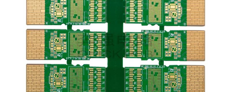
PCB wiring layout tips for beginners
As an electronic engineer, designing circuits is a necessary and hard skill, but no matter how perfect the principle design is, if the circuit board design is unreasonable, the performance will be greatly reduced, and in serious cases, it may not even work properly.
No matter what software is used, there is a general procedure for PCB design. Going in order will save time and effort, so I will introduce it according to the production process. (Because the Protel interface style is close to that of Windows, the operating habits are also similar, and it has powerful simulation functions, so many people use it, so this software will be used as an explanation.)
Schematic design is the preliminary preparation work. It is often seen that beginners directly draw the PCB board to save trouble. This will not be worth the gain. For simple boards, if you are familiar with the process, you may as well skip it. But for beginners, they must follow the process. On the one hand, they can develop good habits. On the other hand, this is the only way to avoid making mistakes with complex circuits.
When drawing schematic diagrams, when designing hierarchies, attention should be paid to the final connection of each file into a whole, which is also of great significance for future work. Due to differences in software, some software may appear to be connected but actually not connected (in terms of electrical performance). If you don’t use relevant testing tools to detect it, if something goes wrong, it will be too late until the board is ready. Therefore, I have repeatedly emphasized the importance of doing it in order, hoping to attract everyone’s attention.
The schematic diagram is based on the designed project. As long as the electrical connections are correct, there is nothing much to say. Below we focus on discussing the specific issues in the board making process.
1. Make physical borders
The closed physical border is a basic platform for future component layout and wiring, and also constrains automatic layout. Otherwise, the components coming from the schematic diagram will be at a loss. But you must pay attention to accuracy here, otherwise you will be in trouble if there are installation problems in the future. In addition, it is best to use arcs at corners. On the one hand, it can avoid sharp corners from scratching workers, and at the same time, it can reduce stress. In the past, one of my products always had the case PCB board broken during transportation. It was fine after using arc.
2. Introduction of components and networks
It should be very simple to introduce components and networks into the drawn borders, but problems often arise here. You must carefully follow the errors prompted to solve them one by one, otherwise you will have to spend more effort later. The problems here generally include the following:
The packaging form of the component cannot be found, there is a component network problem, there are unused components or pins, the comparison prompts that these problems can be solved quickly.
3. Component layout
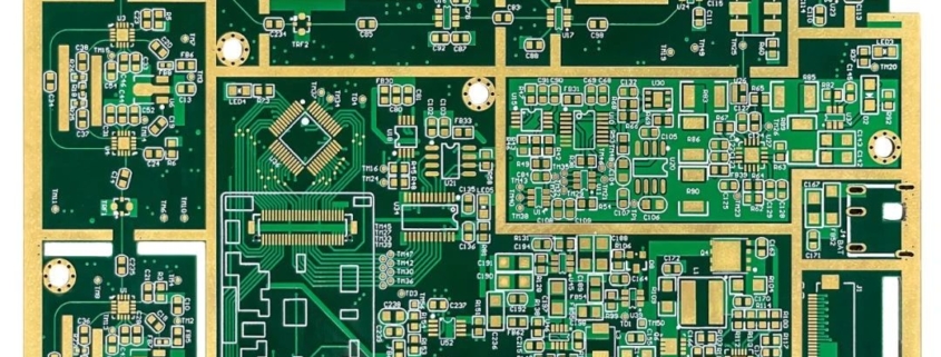
The layout and wiring of components have a great impact on the product’s life, stability, and electromagnetic compatibility, and should be paid special attention to. Generally speaking, there should be the following principles:
(1) Placement order
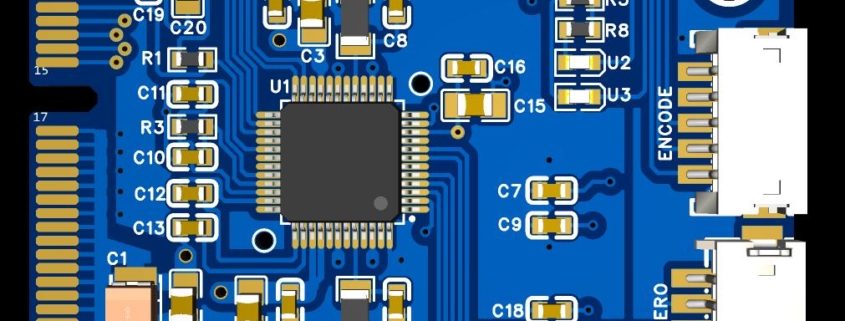
First place the fixed-position components related to the structure, such as power sockets, indicator lights, switches, connectors, etc. After placing these components, use the LOCK function of the software to lock them so that they will not be moved accidentally in the future. Then place special components and large components on the circuit, such as heating components, transformers, ICs, etc. Place the widget last.
(2) Pay attention to heat dissipation
The component layout should also pay special attention to heat dissipation issues. For high-power circuits, heating components such as power tubes and transformers should be placed as far apart as possible to facilitate heat dissipation. Do not concentrate them in one place, and do not have high capacitances too close to avoid premature aging of the electrolyte.
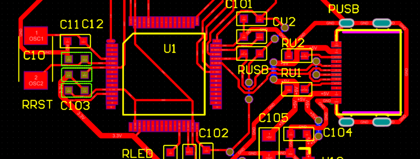
4. wiring
Wiring principles
The knowledge of routing is very profound, and everyone will have their own experience, but there are still some general principles.
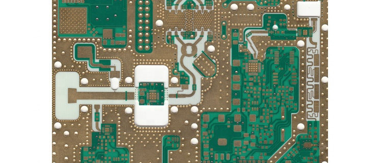
◆It is better for high-frequency digital circuit traces to be thinner and shorter.
◆Attention should be paid to the isolation between large current signals, high voltage signals and small signals (the isolation distance is related to the withstand voltage to be withstood. Normally at 2KV, the distance between the boards should be 2mm, and the distance above this should be increased proportionally. , for example, if it wants to withstand the 3KV withstand voltage test, the distance between high and low voltage lines should be more than 3.5mm. In many cases, in order to avoid creepage, slots are also made between high and low voltage on the printed circuit board.)
◆When wiring two panels, the wires on both sides should be routed perpendicularly, obliquely, or bent to avoid being parallel to each other to reduce parasitic coupling; printed wires used as input and output of the circuit should avoid adjacent parallel lines as much as possible. , to avoid feedback, it is best to add a ground wire between these wires.
◆Make the wiring corners larger than 90 degrees as much as possible, avoid corners below 90 degrees, and use 90-degree corners as little as possible
◆If they are both address lines or data lines, the length of the lines should not be too different, otherwise the short lines will need to be artificially bent to compensate.
◆Try to run the traces on the welding surface as much as possible, especially for PCBs with through-hole technology
◆Use as few vias and jumpers as possible
◆The soldering pads of single-sided panels must be large, and the wires connecting the pads must be thick. Use teardrops if you can. The quality of ordinary single-sided panel manufacturers will not be very good, otherwise there will be problems with welding and RE-WORK.
◆Large areas of copper should be covered in a grid pattern to prevent the board from generating bubbles and bending due to thermal stress during wave soldering. However, in special occasions, the flow direction and size of the GND must be considered, and it cannot simply be filled with copper foil. , but need to route
◆Components and wiring should not be placed too close to the edge. Common single panels are mostly made of paper boards, which are easy to break after being stressed. If you connect wires or place components at the edge, they will be affected.
◆The convenience of production, debugging and maintenance must be considered
It is very important to deal with ground issues for analog circuits. Noise generated on the ground is often unpredictable, but once it occurs, it will cause great trouble and should be avoided. For power amplifier circuits, extremely small ground noise will have a significant impact on the sound quality due to the amplification of the subsequent stages; in high-precision A/D conversion circuits, if there are high-frequency components on the ground line, there will be a certain temperature drift, which will affect the sound quality. Amplifier work. At this time, you can add decoupling capacitors to the 4 corners of the board, connect one leg to the ground on the board, and connect the other leg to the mounting hole (connected to the chassis through screws), so that this component can be eliminated, and the amplifier and AD can also It’s stable.
In addition, the issue of electromagnetic compatibility has become even more important now that people are paying more attention to environmentally friendly products. Generally speaking, there are three sources of electromagnetic signals: signal source, radiation, and transmission line. Crystal oscillator is a common high-frequency signal source. In the power spectrum, the energy value of each harmonic of the crystal oscillator will be significantly higher than the average value. A feasible approach is to control the amplitude of the signal, ground the crystal oscillator shell, shield the interference signal, and use special filter circuits and devices.
What needs special explanation is the snake-shaped wiring, because its functions are different depending on the application. It is used on some clock signals in the computer motherboard, such as PCIClk and AGP-Clk. It has two functions: 1. Impedance matching 2. Filter inductor.
For some important signals, such as the HUBLink in the INTELHUB architecture, there are 13 wires in total and the frequency can reach 233MHZ. They must be strictly equal in length to eliminate the hidden dangers caused by time lag. At this time, snake wiring is the only solution.
Generally speaking, the line spacing of snake-shaped traces is >= 2 times the line width; if it is used in an ordinary PCB board, in addition to having the function of a filter inductor, it can also be used as an inductor coil of a radio antenna, etc.
5. Adjustment and improvement
After completing the wiring, all that needs to be done is to make some adjustments to the text, individual components, and wiring and apply copper (this work should not be done too early, otherwise it will affect the speed and cause trouble to the wiring), also for the convenience of production, Debugging and maintenance.
Copper coating usually refers to filling the blank area left after wiring with a large area of copper foil. You can lay GND copper foil or VCC copper foil (but this will easily burn the device in the event of a short circuit. It is best to ground it unless you have to. To increase the conduction area of the power supply to withstand larger current, connect to VCC). Ground wrapping usually refers to wrapping a bunch of signal lines with special requirements with two ground wires (TRAC) to prevent them from being interfered by or interfering with others.
If you use copper instead of ground wire, you must pay attention to whether the entire ground is connected, the current size, flow direction, and whether there are any special requirements to ensure that unnecessary mistakes are reduced.
6. Check the network
Sometimes due to misoperation or negligence, the network relationship of the drawn board is different from the schematic diagram. In this case, it is necessary to check. Therefore, after finishing the painting, you must not rush to hand it over to the plate maker. You should check it first and then proceed with the follow-up work.
7. Use the simulation function
After completing these tasks, if time permits, software simulation can also be performed. Especially for high-frequency digital circuits, some problems can be discovered in advance and greatly reduce the workload of debugging in the future.
As an electronic engineer, designing circuits is a necessary and hard skill, but no matter how perfect the principle design is, if the circuit board design is unreasonable, the performance will be greatly reduced, and in serious cases, it may not even work properly. Based on my experience, I have summarized the following things that should be paid attention to in PCB design. I hope it can inspire you.
No matter what software is used, there is a general procedure for PCB design. Going in order will save time and effort, so I will introduce it according to the production process. (Because the Protel interface style is close to that of Windows, the operating habits are also similar, and it has powerful simulation functions, so many people use it, so this software will be used as an explanation.)
Schematic design is the preliminary preparation work. It is often seen that beginners directly draw the PCB board to save trouble. This will not be worth the gain. For simple boards, if you are familiar with the process, you may as well skip it. But for beginners, they must follow the process. On the one hand, they can develop good habits. On the other hand, this is the only way to avoid making mistakes with complex circuits.
When drawing schematic diagrams, when designing hierarchies, attention should be paid to the final connection of each file into a whole, which is also of great significance for future work. Due to differences in software, some software may appear to be connected but actually not connected (in terms of electrical performance). If you don’t use relevant testing tools to detect it, if something goes wrong, it will be too late until the board is ready. Therefore, I have repeatedly emphasized the importance of doing it in order, hoping to attract everyone’s attention.
The schematic diagram is based on the designed project. As long as the electrical connections are correct, there is nothing much to say. Below we focus on discussing the specific issues in the board making process.
1. Make physical borders
The closed physical border is a basic platform for future component layout and wiring, and also constrains automatic layout. Otherwise, the components coming from the schematic diagram will be at a loss. But you must pay attention to accuracy here, otherwise you will be in trouble if there are installation problems in the future. In addition, it is best to use arcs at corners. On the one hand, it can avoid sharp corners from scratching workers, and at the same time, it can reduce stress. In the past, one of my products always had the case PCB board broken during transportation. It was fine after using arc.
2. Introduction of components and networks
It should be very simple to introduce components and networks into the drawn borders, but problems often arise here. You must carefully follow the errors prompted to solve them one by one, otherwise you will have to spend more effort later. The problems here generally include the following:
The packaging form of the component cannot be found, there is a component network problem, there are unused components or pins, the comparison prompts that these problems can be solved quickly.
3. Component layout
The layout and wiring of components have a great impact on the product’s life, stability, and electromagnetic compatibility, and should be paid special attention to. Generally speaking, there should be the following principles:
(1) Placement order
First place the fixed-position components related to the structure, such as power sockets, indicator lights, switches, connectors, etc. After placing these components, use the LOCK function of the software to lock them so that they will not be moved accidentally in the future. Then place special components and large components on the circuit, such as heating components, transformers, ICs, etc. Place the widget last.
(2) Pay attention to heat dissipation
The component layout should also pay special attention to heat dissipation issues. For high-power circuits, heating components such as power tubes and transformers should be placed as far apart as possible to facilitate heat dissipation. Do not concentrate them in one place, and do not have high capacitances too close to avoid premature aging of the electrolyte.
4. wiring
Wiring principles
The knowledge of routing is very profound, and everyone will have their own experience, but there are still some general principles.
◆It is better for high-frequency digital circuit traces to be thinner and shorter.
◆Attention should be paid to the isolation between large current signals, high voltage signals and small signals (the isolation distance is related to the withstand voltage to be withstood. Normally at 2KV, the distance between the boards should be 2mm, and the distance above this should be increased proportionally. , for example, if it wants to withstand the 3KV withstand voltage test, the distance between high and low voltage lines should be more than 3.5mm. In many cases, in order to avoid creepage, slots are also made between high and low voltage on the printed circuit board.)
◆When wiring two panels, the wires on both sides should be routed perpendicularly, obliquely, or bent to avoid being parallel to each other to reduce parasitic coupling; printed wires used as input and output of the circuit should avoid adjacent parallel lines as much as possible. , to avoid feedback, it is best to add a ground wire between these wires.
◆Make the wiring corners larger than 90 degrees as much as possible, avoid corners below 90 degrees, and use 90-degree corners as little as possible
◆If they are both address lines or data lines, the length of the lines should not be too different, otherwise the short lines will need to be artificially bent to compensate.
◆Try to run the traces on the welding surface as much as possible, especially for PCBs with through-hole technology
◆Use as few vias and jumpers as possible
◆The soldering pads of single-sided panels must be large, and the wires connecting the pads must be thick. Use teardrops if you can. The quality of ordinary single-sided panel manufacturers will not be very good, otherwise there will be problems with welding and RE-WORK.
◆Large areas of copper should be covered in a grid pattern to prevent the board from generating bubbles and bending due to thermal stress during wave soldering. However, in special occasions, the flow direction and size of the GND must be considered, and it cannot simply be filled with copper foil. , but need to route
◆Components and wiring should not be placed too close to the edge. Common single panels are mostly made of paper boards, which are easy to break after being stressed. If you connect wires or place components at the edge, they will be affected.
◆The convenience of production, debugging and maintenance must be considered
It is very important to deal with ground issues for analog circuits. Noise generated on the ground is often unpredictable, but once it occurs, it will cause great trouble and should be avoided. For power amplifier circuits, extremely small ground noise will have a significant impact on the sound quality due to the amplification of the subsequent stages; in high-precision A/D conversion circuits, if there are high-frequency components on the ground line, there will be a certain temperature drift, which will affect the sound quality. Amplifier work. At this time, you can add decoupling capacitors to the 4 corners of the board, connect one leg to the ground on the board, and connect the other leg to the mounting hole (connected to the chassis through screws), so that this component can be eliminated, and the amplifier and AD can also It’s stable.
In addition, the issue of electromagnetic compatibility has become even more important now that people are paying more attention to environmentally friendly products. Generally speaking, there are three sources of electromagnetic signals: signal source, radiation, and transmission line. Crystal oscillator is a common high-frequency signal source. In the power spectrum, the energy value of each harmonic of the crystal oscillator will be significantly higher than the average value. A feasible approach is to control the amplitude of the signal, ground the crystal oscillator shell, shield the interference signal, and use special filter circuits and devices.
What needs special explanation is the snake-shaped wiring, because its functions are different depending on the application. It is used on some clock signals in the computer motherboard, such as PCIClk and AGP-Clk. It has two functions: 1. Impedance matching 2. Filter inductor.
For some important signals, such as the HUBLink in the INTELHUB architecture, there are 13 wires in total and the frequency can reach 233MHZ. They must be strictly equal in length to eliminate the hidden dangers caused by time lag. At this time, snake wiring is the only solution.
Generally speaking, the line spacing of snake-shaped traces is >= 2 times the line width; if it is used in an ordinary PCB board, in addition to having the function of a filter inductor, it can also be used as an inductor coil of a radio antenna, etc.
5. Adjustment and improvement
After completing the wiring, all that needs to be done is to make some adjustments to the text, individual components, and wiring and apply copper (this work should not be done too early, otherwise it will affect the speed and cause trouble to the wiring), also for the convenience of production, Debugging and maintenance.
Copper coating usually refers to filling the blank area left after wiring with a large area of copper foil. You can lay GND copper foil or VCC copper foil (but this will easily burn the device in the event of a short circuit. It is best to ground it unless you have to. To increase the conduction area of the power supply to withstand larger current, connect to VCC). Ground wrapping usually refers to wrapping a bunch of signal lines with special requirements with two ground wires (TRAC) to prevent them from being interfered by or interfering with others.
If you use copper instead of ground wire, you must pay attention to whether the entire ground is connected, the current size, flow direction, and whether there are any special requirements to ensure that unnecessary mistakes are reduced.
6. Check the network
Sometimes due to misoperation or negligence, the network relationship of the drawn board is different from the schematic diagram. In this case, it is necessary to check. Therefore, after finishing the painting, you must not rush to hand it over to the plate maker. You should check it first and then proceed with the follow-up work.
7. Use the simulation function
After completing these tasks, if time permits, software simulation can also be performed. Especially for high-frequency digital circuits, some problems can be discovered in advance and the future debugging workload can be greatly reduced.