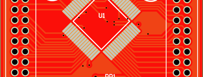
Starting from PCB design, signal integrity is no longer difficult!

In the world of electronics design, high-performance design has its own unique challenges.

1 The birth of high-speed design

In recent years, the increasing number of high-frequency signal designs has been closely linked to the steadily increasing performance of electronic systems.

As system performance improves, the challenges for PCB designers are increasing day by day: smaller chips, denser circuit board layout, and lower power consumption chip requirements.

With the rapid development of all technologies, we are at the core of high-speed design and need to consider its complexity and all factors.

2 review

PCB design has changed a lot over the past 30 years. In 1987, we thought 0.5 micron was the end of the technology, but today, 22nm has become the norm.

As shown in the figure below, the edge rate in 1985 promoted the increase in design complexity (typically 30 nanoseconds), and today the edge rate has become 1 nanosecond.
图片

Changes in marginal rates over the past 30 years.

3 Technological progress is accompanied by various problems

The advancement of technology is always accompanied by a series of problems. As system performance increases and high-speed designs are adopted, some issues must be addressed in the design environment.

Below, we summarize the challenges faced:

Signal quality

IC manufacturers favor lower core voltages and higher operating frequencies, which results in sharply rising edge rates. Edge rates in unterminated designs will cause reflections and signal quality issues.

crosstalk

In high-speed signal designs, dense paths often lead to crosstalk—the phenomenon associated with electromagnetic coupling between traces on a PCB.

Crosstalk can be edge coupling of traces on the same layer or broadside coupling on adjacent layers.

The coupling is three-dimensional. Parallel paths and wide-side traces cause more crosstalk than side-by-side trace paths.

图片

Broadside coupling (top) compared to edge coupling (bottom)

Fast edge rates in traditional designs can cause ringing on unterminated transmission lines, even when using the same frequency and trace length as before.

This essentially results in higher emissions, well in excess of the FCC/CISPR Class B limits for unterminated transmission lines.

图片

Edge rate radiation at 10 nanoseconds (left) and 1 nanosecond (right).

4 Design Solutions

Signal and power integrity issues occur intermittently and are difficult to diagnose. Therefore, the best way is to find the root cause of the problem during the design process and eliminate it, rather than trying to solve it in the later stages and delaying production.

The stackup planning tool makes it easier to implement solutions to signal integrity issues in your design.

5 Circuit board stackup planning

The number one priority in high-speed design must be circuit board stackup. The substrate is the most important component of the assembly, and its specifications must be carefully planned to avoid discontinuous impedance, signal coupling, and excessive electromagnetic radiation.

When looking at the circuit board stackup for your next design, keep these tips and suggestions in mind:
All signal layers need to be adjacent and tightly coupled to an uninterrupted reference plane that creates a clear loop and eliminates broadside crosstalk.

图片

The substrate of each signal layer is adjacent to the reference plane.

There are good planar capacitors to reduce AC impedance in high frequencies. The tightly coupled inner electrical layer plane reduces the AC impedance of the top layer and greatly reduces electromagnetic radiation.

Reducing the dielectric height significantly reduces crosstalk without impacting the available space on the board.

The substrate should be able to accommodate a range of different technologies. For example: 50/100 ohm digital, 40/80 ohm DDR4, 90 ohm USB.

6 Cabling and Workflow

With your stackup carefully planned, the next step is to focus on board routing. Based on design rules and careful configuration of your work area, you can route your board most efficiently and successfully.

These tips can help make your wiring easier and avoid unnecessary crosstalk, radiation, and signal quality problems:

Simplify the view to clearly see the split planes and current loops.

To do this, first determine which copper foil plane (ground or power) serves as the reference plane for each signal layer, and then open the signal layer and internal electrical layer planes to view them at the same time. This helps you more easily see the traces that split the plane.

图片

Multiple signal layers (left), top and adjacent plane views (right)

If a digital signal must cross a power reference plane, you can place one or two decoupling capacitors (100nF) close to the signal. This provides a current loop between the two power supplies.

Avoid parallel routing and broadside routing, which can cause more crosstalk than side-by-side routing.

Unless you are using a synchronous bus, keep the parallel intervals as short as possible to reduce crosstalk. Leave room for signal groups so that their address and data spacing is three times the trace width.

Be careful when using combined microstrip layers on the top and bottom layers of the board. This can lead to crosstalk between traces on adjacent board layers, compromising signal integrity.

Routing the clock (or strobe) signal with the longest delay by signal group ensures that the data has been established before the clock is read.

Routing embedded signals between planes helps minimize radiation and provides ESD protection.

7 Signal clarity

In the future, the complexity of electronic design will undoubtedly continue to increase, which will bring a series of challenges to PCB designers that need to be solved. Ensuring the correct configuration of circuit board stackup, impedance, and current loops is the basis for design stability.

High-speed PCB board material selection guide: how to make the best decision?

In modern electronic equipment, high-speed PCB circuit boards are increasingly used. In order to achieve higher signal transmission rates and lower signal loss, it is crucial to select the appropriate board material. This article will introduce you to some factors to help you make the correct PCB board material selection decision to ensure the stability and optimization of circuit performance.

1. Understand the characteristics of high-speed PCB boards
Before choosing high-speed PCB boards, you first need to understand the characteristics of different boards. Common high-speed PCB boards include FR-4, PTFE, Rogers, etc. Each type of plate has different characteristics such as dielectric constant, thermal expansion coefficient, and temperature resistance. When selecting a board material, you need to determine which properties are more important based on the needs of the specific application.

2. Consider signal transmission rate
High-speed PCB circuit boards usually need to transmit high-frequency signals, so the dielectric constant of the board is crucial to the signal transmission rate. A lower dielectric constant can reduce signal propagation delays and losses and improve circuit performance. Therefore, choosing a plate with a lower dielectric constant is a wise choice.

3. Consider the thermal expansion coefficientThe coefficient of thermal expansion refers to the degree of dimensional change of a material when the temperature changes. In high-speed PCB circuit board design, temperature changes may cause dimensional changes in the board, thereby affecting the stability of the circuit. Therefore, choosing a sheet with a smaller coefficient of thermal expansion can reduce problems caused by temperature changes.

4. Consider temperature resistance
High-speed PCB circuit boards usually need to operate at higher temperatures, so the temperature resistance of the board is also a key consideration. Choosing boards with higher temperature resistance can ensure the reliability and stability of the circuit in high-temperature environments.

5. Work with suppliers
When selecting high-speed PCB board materials, it is very important to work with reliable suppliers. They can provide you with professional advice and technical support, and provide high-quality boards that meet quality standards. Establishing long-term relationships with suppliers ensures you receive ongoing technical support and quality products.

Choosing the right high-speed PCB board material is crucial to the stability and optimization of circuit performance. When selecting materials, factors such as the characteristics of the board, signal transmission rate, thermal expansion coefficient, and temperature resistance need to be considered. It is also important to work with reliable suppliers and obtain professional advice and support. By carefully considering these factors, you will be able to make the correct PCB board material selection decision, improving your circuit performance and overall product quality.

How to use high-speed PCB prototyping to improve product performance?

In the rapid development of modern electronic products, high-speed PCB proofing has become a key part of improving product performance. This article will introduce to you how to improve product performance through high-speed PCB proofing.

1. Understand the concept and significance of high-speed pcb prototyping
In electronic product design, high-speed PCB prototyping refers to the use of high-performance materials, precision processes and advanced equipment when designing and manufacturing PCB boards to meet high-speed signal transmission, anti-interference ability and stability requirements. Through high-speed PCB prototyping, signal transmission delay and signal distortion can be effectively reduced, and the reliability and stability of the product can be improved.

2. Choose suitable high-speed PCB materials
Choosing suitable high-speed PCB materials is an important step to ensure product performance improvement. Common high-speed PCB materials include FR-4, Rogers, PTFE, etc. According to the specific needs of the product, the dielectric constant, loss factor and thermal stability of the material are selected to meet the requirements of high-speed signal transmission.

3. Optimize PCB layout and routing
When performing high-speed PCB prototyping, reasonable layout and wiring design can significantly improve product performance. Try to shorten the signal transmission path as much as possible to reduce signal loss; avoid excessive plane layering to reduce signal crosstalk and interference. In addition, the ground wire and power wire should be properly set up to provide good ground potential and power supply stability.

4. Pay attention to the details in high-speed PCB proofing
When performing high-speed PCB prototyping, you also need to pay attention to some details to ensure the improvement of product performance. Choose the appropriate PCB manufacturer to ensure that it has advanced production equipment and rich experience; conduct strict process control, including controlling the accuracy of parameters such as board thickness, line width, line spacing; and conduct necessary testing and verification to ensure that the product The quality and performance meet expectations.

Using high-speed PCB proofing can significantly improve product performance, thereby achieving better user experience and market competitiveness. By choosing the right materials, optimizing layout and trace design, and paying attention to detail and process control, you can maximize product performance.

Revealing the difference between high-frequency PCB and ordinary PCB, do you really understand it?

In the electronics industry, PCB (Printed Circuit Board) is an important component, which carries electronic components and provides connection functions. In the world of PCB, high-frequency PCB and ordinary PCB are two common concepts. However, do you really know the difference between them? This article will reveal the differences between high-frequency PCBs and ordinary PCBs to help you understand them better.

Material selection: High-frequency PCB requires the use of special materials with low dielectric constant and low loss tangent to support higher frequency signal transmission and faster data processing. Ordinary PCBs may use conventional FR-4 materials or other more common materials.
Hierarchical structure: High-frequency PCBs may adopt more hierarchical structures to achieve complex signal stacking and impedance matching. In comparison, a normal PCB may require less hierarchical structure.

Layout and wiring: The layout and wiring of high-frequency PCBs need to be more precise and rigorous to minimize signal path length, signal distortion and crosstalk. The layout and wiring of ordinary PCB may be relatively more flexible and simple.

Impedance control: High-frequency PCBs need to strictly control the impedance matching of signal transmission lines to ensure stable signal transmission. In comparison, ordinary PCBs may have less stringent requirements for impedance control.

Testing requirements: The testing requirements for high-frequency PCBs are more stringent, and more advanced testing equipment and technologies are usually required to ensure the accuracy and stability of signal transmission. The testing requirements for ordinary PCBs may be relatively simple and straightforward.

Cost and manufacturing process: Because high-frequency PCBs have higher requirements on materials, processes, and testing, manufacturing costs may be higher. The manufacturing cost of ordinary PCB is relatively low, and the manufacturing process is relatively simple.

In general, there are some differences between high-frequency PCBs and ordinary PCBs in terms of material selection, hierarchical structure, layout and wiring, impedance control, testing requirements and manufacturing costs. High-frequency PCBs are more specialized and complex and are suitable for application scenarios with higher signal transmission requirements, while ordinary PCBs are more versatile and suitable for general electronic product manufacturing. By understanding these differences, it helps us better select and apply suitable PCBs and improve the performance and stability of electronic equipment.

Why is it important to understand the pros and cons of high frequency microwave circuit boards?

High-frequency microwave circuit board is a circuit board specially used for high-frequency microwave signal transmission, which has unique advantages and limitations. By understanding its advantages and disadvantages, we can better apply and optimize this circuit board and improve product quality and performance.

First, let us understand the advantages of high frequency microwave circuit boards. High-frequency microwave PCB circuit board has excellent high-frequency characteristics and can show lower signal loss and higher signal transmission efficiency in high-frequency microwave signal transmission. In addition, it also has good anti-interference performance and can effectively resist the impact of external interference on signal transmission. In addition, the manufacturing process of high-frequency microwave PCB circuit boards is relatively mature and can meet the needs of mass production.

However, high-frequency microwave circuit boards also have some limitations. First, its manufacturing process is relatively complex and requires highly precise processing and production equipment, so it is prone to process challenges during the production process. High-frequency microwave circuit boards have higher material requirements and require the use of specific high-frequency materials, which also increases the cost and manufacturing difficulty. In addition, high-frequency microwave PCB circuit boards need to consider more high-frequency characteristics in the design and layout, and the technical requirements for designers are also higher.

Understanding the advantages and disadvantages of high-frequency microwave PCB circuit boards is crucial for the electronics industry and communications field. Only by fully understanding its advantages and disadvantages can we better apply and optimize this circuit board and improve product quality and performance. Through targeted optimization and improvement, we can better meet the needs of high-frequency microwave signal transmission and provide more reliable technical support for development and innovation in the communications field.

What is a rigid printed circuit board?

In today’s era of rapid technological development, rigid printed circuit boards have become an indispensable part of electronic products. So, what exactly is a rigid printed circuit board?

What is a rigid printed circuit board?

Rigid printed circuit board is an electronic component composed of an insulating substrate, a conductor layer and a copper clad layer. Compared with flexible printed circuit boards, the main feature of rigid printed circuit boards is that the substrate material is usually fiberglass laminated board or epoxy resin board, which has high mechanical strength and stability.
Characteristics of rigid printed circuit boards
High mechanical strength: Rigid printed circuit boards use solid substrate materials and have high mechanical strength, making them suitable for electronic products with high stability requirements.

Good thermal stability: Rigid printed circuit boards can maintain stable performance at higher temperatures and are suitable for electronic equipment in high-temperature environments.

Easy to assemble: The structure of the rigid printed circuit board is stable, which facilitates the welding and assembly of components and improves production efficiency.

Excellent electrical performance: The distance between the conductor layers of the rigid printed circuit board is short, the signal transmission speed is fast, and the electrical performance is excellent.
Application areas of rigid printed circuit boards

Rigid printed circuit boards are widely used in various electronic products, including but not limited to:
Computer and communication equipment: Rigid printed circuit boards are required in electronic equipment such as motherboards, routers, switches, etc.

Consumer electronics: Consumer electronics such as smartphones, tablets, digital cameras, etc. also require rigid printed circuit boards to support their functionality.

Industrial control equipment: Rigid printed circuit boards are also widely used in industrial automation equipment, robots and other fields.

Medical equipment: Rigid printed circuit boards are also commonly used in medical equipment such as medical imaging equipment and electrocardiographs.
As an important component of electronic products, rigid printed circuit boards play an irreplaceable role in various fields, providing important support for the stable operation and efficient performance of electronic equipment.

How to prevent PCBA circuit boards from bending and warping during reflow soldering?

1. Reduce the impact of temperature on circuit board stress

Since “temperature” is the main source of circuit board stress, as long as the temperature of the reflow oven is lowered or the speed of heating and cooling of the circuit board in the reflow oven is slowed down, the bending and warping of the board can be greatly reduced. occur. However, other side effects may occur, such as solder short circuits.

2. PCB uses high Tg board

Tg is the glass transition temperature, which is the temperature at which the material changes from glass to rubber. The lower the Tg value of the material, the faster the circuit board begins to soften after entering the reflow oven and becomes soft and rubbery. The time will also become longer, and the deformation of the circuit board will of course become more serious. Using a higher Tg board can increase its ability to withstand stress deformation, but the price of high Tg PCB boards is relatively high.

3. Increase the thickness of the circuit board

In order to make many electronic products thinner and lighter, the thickness of the circuit board has been reduced to 1.0mm, 0.8mm, or even 0.6mm. Such a thickness is really a bit difficult to keep the circuit board from deforming after passing through the reflow oven. It is difficult to force people to do so. It is recommended that if there is no requirement to be thin and light, the circuit board should be 1.6mm thick, which can greatly reduce the risk of board bending and deformation.

4. Reduce the size of the circuit board and reduce the number of panels

Since most reflow ovens use chains to drive the circuit board forward, circuit boards with larger PCB design sizes will be dented and deformed in the reflow oven due to their own weight, so try to treat the long side of the circuit board as the board edge. Putting it on the chain of the reflow furnace can reduce the dent deformation caused by the weight of the circuit board itself. This is also the reason for reducing the number of panels. That is to say, when passing through the furnace, try to use the narrow edge perpendicular to the furnace passing direction. Achieve the lowest amount of dent deformation.

5. Use oven tray jig

If the above methods are difficult to achieve, the last option is to use an oven tray to reduce the amount of deformation. The reason why the oven tray can reduce the bending of the board is because whether it is thermal expansion or cold contraction, the tray is expected to be able to fix the circuit board. When the temperature of the circuit board drops below the Tg value and begins to harden again, the original size can be maintained.

If the single-layer pallet cannot reduce the deformation of the circuit board, you must add a layer of cover and clamp the circuit board with the upper and lower pallets. This can greatly reduce the problem of deformation of the circuit board after passing through the reflow oven. However, these oven trays are quite expensive, and labor is required to place and recycle the trays.

What are the parameters of the circuit board?

PCB circuit board parameters

1. ∑ Dielectric constant (DK value): Usually represents the ability of a certain material to store electrical energy. The smaller the ∑ value, the smaller the ability to store electrical energy and the faster the transmission speed.

2. TG (glass transition temperature): When the temperature rises to a certain area, the substrate will change from “glass state” to “rubber state”. The temperature point at this time is called the glass transition temperature (Tg) of the board. Tg is the maximum temperature (℃) at which the substrate remains “rigid”.

3. CTI (Current Tracking Resistance Index): Indicates the quality of insulation. The larger the CTI value, the better the insulation.

4. TD (thermal decomposition temperature): an important indicator to measure the heat resistance of the plate.

5. CTE (Z-axis) – (Z-axis thermal expansion coefficient): a performance index that reflects the decomposition of thermal expansion of the plate. The smaller the CTE value, the better the performance of the plate.

PCB board knowledge and standards

At present, there are many classification methods for copper-clad laminates that are widely used in our country. Generally, according to the reinforcing materials of the board, it can be divided into five categories: paper base, glass fiber cloth base, composite base (CEM series), laminated multi-layer board base and special material base (ceramic, metal core base, etc.). If classified according to the resin adhesive used in the board, common paper-based CCI include: phenolic resin (XPc, XxxPC, FR-1, FR-2, etc.), epoxy resin (FE-3), polyester Resin and other types. Common fiberglass cloth-based CCLs include epoxy resin (FR-4, FR-5), which is currently the most widely used fiberglass cloth-based type.

There are also other special resins (using glass fiber cloth, polyamide fiber, non-woven fabric, etc. as additional materials): bismaleimide-modified triazine resin (BT), polyimide resin (PI) , diphenylene ether resin (PPO), maleic anhydride imine-styrene resin (MS), polycyanate resin, polyolefin resin, etc. According to the flame retardant performance of CCL, it can be divided into two types of boards: flame retardant type (UL94-VO, UL94-V1 level) and non-flame retardant type (UL94-HB level). In the past year or two, as countries have paid more and more attention to environmental protection issues, a new type of CCL that does not contain bromine has been divided into flame-retardant CCL, which is generally called “green flame-retardant CCL” . With the rapid development of electronic product technology, the requirements for CCL have become higher.

Therefore, from the performance classification of CCL, it is divided into general performance CCL, low dielectric constant CCL, high heat resistance CCL (generally the L of the board is above 150°C), and low thermal expansion coefficient CCL (generally used on packaging substrates). ) and other types. With the development and continuous progress of electronic technology, new requirements are constantly put forward for PCB substrate materials, thus promoting the continuous development of copper-clad laminate standards. Currently, the main standards for substrate materials are as follows:

① National standards: my country’s national standards for substrate materials include GB/T4721-47221992 and GB4723-4725-1992. The copper-clad laminate standard in Taiwan is the CNS standard, which was formulated based on the Japanese JIs standard in 1983. release.

② International standards: Japanese JIS standards, American ASTM, NEMA, MIL, IPc, ANSI, UL standards, British Bs standards, German DIN, VDE standards, French NFC, UTE standards, Canadian CSA standards, Australian AS standards, FOCT standards of the former Soviet Union, international IEC standards, etc.; common and commonly used suppliers of PCB design materials include: Shengyi\Kingboard\International, etc.

PCB boards are divided according to brand quality level from bottom to top as follows: 94HB-94VO-CEM-1-CEM-3-FR-4

Its specific parameters and uses are as follows:

94HB: Ordinary cardboard, not fireproof (the lowest grade material, die-punched, cannot be used as a power board)

94V0: Flame retardant cardboard (die punching)

22F: Single-sided semi-fiberglass board (die punching)

CEM-1: Single-sided fiberglass board (must be computer drilled, not punched)

CEM-3: Double-sided semi-glass fiber board (except for double-sided cardboard, it is the lowest-end material for double-sided panels. Simple double-sided panels can use this material, which is 5~10 yuan/square meter cheaper than FR-4)

FR-4: Double-sided fiberglass board

1. The classification of flame retardant properties can be divided into four types: 94VO-V-1 -V-2 -94HB

2. Pre-cured sheet: 1080=0.0712mm, 2116=0.1143mm, 7628=0.1778mm

3. FR4 CEM-3 both represent boards, fr4 is fiberglass board, and cem3 is composite substrate

4. Halogen-free refers to substrates that do not contain halogens (fluorine, bromine, iodine and other elements), because bromine produces toxic gases when burned.

5. Tg is the glass transition temperature, that is, the melting point.

6. The circuit board must be flame-resistant and cannot burn at a certain temperature, but can only soften. The temperature point at this time is called the glass transition temperature (Tg point). This value is related to the dimensional durability of the PCB board.

What is high Tg? PCB circuit board and the advantages of using high Tg PCB

High Tg refers to high heat resistance. When the temperature of a high Tg pcb circuit board rises to a certain threshold, the substrate will change from “glass state” to “rubber state”. The temperature at this time is called the board The glass transition temperature (Tg). Equivalently, Tg is the maximum temperature (°C) at which the base material remains rigid. That is, ordinary PCB circuit board substrate materials continue to soften, deform, melt, etc. under high temperatures. At the same time, they also show a sharp decline in mechanical and electrical properties, which affects the service life of the product. Usually Tg boards is above 130°C, high Tg is usually greater than 170°C, and medium Tg is about greater than 150°C; PCB circuit boards with Tg ≥ 170°C are usually called high Tg PCB; the Tg of the substrate is increased, and the heat resistance and moisture resistance of the circuit board are improved , chemical resistance, resistance and stability and other characteristics will be improved and improved. The higher the TG value, the better the temperature resistance of the board. Especially in lead-free processes, there are many high Tg applications.

With the rapid development of the electronics industry, especially electronic products represented by computers, which are developing towards high functionality and high multi-layering, higher heat resistance of PCB circuit board substrate materials is required as a prerequisite. The emergence and development of high-density mounting technologies represented by SMT and CMT have made PCB circuit boards increasingly inseparable from the support of high heat resistance of the substrate in terms of small aperture, fine wiring, and thinness.

Therefore, the difference between ordinary FR-4 and high Tg is: at high temperatures, especially when heated after absorbing moisture, the mechanical strength, dimensional stability, adhesion, water absorption, thermal decomposition, and thermal expansion of the material There are certain differences in different situations. High Tg products are obviously much better than ordinary PCB circuit board substrate materials.

What are the important parameters of high-frequency PCB?

The dielectric constant (Dk) of the high-frequency circuit board substrate must be small and stable. Generally speaking, the smaller the better. The signal transmission rate is inversely proportional to the square root of the material’s dielectric constant. A high dielectric constant can easily cause signal transmission delays. .

The dielectric loss (Df) of high-frequency circuit board substrate materials must be small, which mainly affects the quality of signal transmission. The smaller the dielectric loss, the smaller the signal loss.

The impedance of high-frequency circuit boards actually refers to the parameters of resistance and reactance. Since PCB circuits must consider the insertion and installation of electronic components, and consider issues such as conductive performance and signal transmission performance after plugging, the lower the impedance, the better. .

The base material of high-frequency circuit boards should have low water absorption. High water absorption will cause dielectric constant and dielectric loss when it gets wet.

In order to meet the signal integrity requirements of different applications, PCB not only needs to test S parameters and TDR impedance, but also needs to analyze the physical properties of the material itself, dielectric constant and dielectric loss. An accurate dielectric constant can not only achieve effective design, but also make simulation and product real test results more consistent, improve the efficiency of design and development, and is of great significance to PCB material suppliers, including PCB production developers.

What are the PCB design requirements?

Today’s PCB technology mainly changes according to the characteristics and requirements of electronic products. In recent years, electronic products have become increasingly multi-functional, sophisticated and comply with environmental regulations. Therefore, the precision of PCB is getting higher and higher, and its application of combining soft and hard boards will also increase.

PCB is the foundation of the information industry. From computers to portable electronic devices, circuit boards are found in almost all electronic and electrical products. With the development of communication technology, handheld wireless radio frequency circuit technology is used more and more widely. One of the biggest characteristics of these devices (such as mobile phones, wireless PDAs, etc.) is: first, they include almost all portable subsystems; second, they are small Miniaturization means that the density of components is very high, which makes the mutual interference of components (including SMD, SMC, bare chips, etc.) very prominent. Therefore, it has become a very important topic to design a perfect PCB for RF circuits and audio circuits to prevent and suppress electromagnetic interference and thereby improve electromagnetic compatibility.

Because the performance indicators of the same circuit and different PCB design structures will vary greatly. Especially as the audio functions of today’s handheld products continue to increase, more attention must be paid to the PCB layout of the audio circuit. Based on this, this article focuses on the ingenious design of the PCB of the RF circuit and audio circuit of the handheld product (that is, including component layout, component arrangement, wiring and Grounding and other techniques) for analysis and explanation.

1. Component layout

First, let’s talk about the general principles of layout: components should be arranged in the same direction as much as possible, and the phenomenon of poor welding can be reduced or even avoided by choosing the direction in which the PCB enters the tin melting system; as known from practice, there must be at least 0.5mm spacing between components to meet the requirements of the components. Regarding the soldering requirements of the device, if the space of the PCB board allows, the spacing between components should be as wide as possible. For double-sided panels, one side should generally be designed with SMD and SMC components, and the other side should be designed with discrete components.

1.1 Divide the PCB into digital areas and analog areas.

The first step in any PCB design is, of course, choosing the PCB placement of each component. We call this step “layout consideration”. Careful component placement can reduce signal interconnections, ground separation, noise coupling, and occupied circuit board area.

Electromagnetic compatibility requires that each circuit module PCB is designed to produce as little electromagnetic radiation as possible and to have a certain anti-electromagnetic interference capability. Therefore, the layout of components also directly affects the interference and anti-interference capabilities of the circuit itself, which is also directly related to performance of the designed circuit.

Therefore, when designing an RF circuit PCB, in addition to considering the layout of ordinary PCB designs, you must also consider how to reduce the mutual interference between various parts of the RF circuit, how to reduce the interference of the circuit itself to other circuits, and the circuit itself. anti-interference ability.

It is known from experience that the quality of the RF circuit effect not only depends on the performance indicators of the RF circuit board itself, but also largely depends on the interaction with the CPU processing board. Since RF circuits contain digital circuits and analog circuits, in order to prevent digital noise from interfering with sensitive analog circuits, they must be separated. Dividing the PCB into digital areas and analog areas can help improve the layout of such circuits, which is particularly important. important.

1.2 Need to prevent RF noise from coupling into audio circuits

Although the RF portion of handheld products is often treated as analog circuitry, a common concern in many designs is RF noise. It is necessary to prevent RF noise from coupling into the audio circuitry, because the RF noise is demodulated to produce audible noise. In order to solve this problem, the RF circuit and the audio circuit need to be separated as much as possible. After dividing the PCB into analog and digital, the component layout of the analog part needs to be considered. The component layout should make the path of the audio signal the shortest, and the audio amplifier should be placed as close as possible to the headphone jack and speaker to minimize the EMI radiation of the Class D audio amplifier and the coupling noise of the headphone signal. The analog audio signal source must be as close as possible to the input of the audio amplifier to minimize input coupling noise. All input leads act as an antenna for RF signals, and shortening the lead length helps reduce the antenna radiation effect in the corresponding frequency band.

2. Issues that should be paid attention to in component layout and application examples

2.1 Issues that should be paid attention to in layout:

Carefully analyze the circuit structure. Divide circuits into blocks (such as high-frequency amplification circuits, mixing circuits and demodulation circuits, etc.) to separate strong current signals and weak current signals as much as possible. After separating digital signal circuits and analog signal circuits, attention should also be paid to Circuits that perform the same function should be arranged within a certain range as much as possible to reduce the signal loop area; the filter network of each part of the circuit must be connected nearby, which can not only reduce radiation, but also reduce the chance of interference and improve the efficiency of the circuit. anti-interference ability.

Unit circuits are grouped according to their different sensitivity to electromagnetic compatibility during use. For components in the circuit that are susceptible to interference, the layout should also try to avoid interference sources (such as interference from the CPU on the data processing board, etc.).

2.2 Examples of the impact of component placement on audio signals

The impact of unreasonable component layout on audio signal quality

An unreasonable layout of audio components has two serious problems: one is that the audio amplifier is too far away from the audio signal source, because the leads pass near noisy digital circuits and switching circuits, thereby increasing the probability of noise coupling. Longer leads also enhance the RF antenna effect. If a mobile phone uses GSM technology, these antennas can pick up the GSM transmitted signal and feed it into the audio amplifier. Almost all amplifiers can demodulate the 217Hz envelope to some extent, producing noise at the output. In the worst case, the noise may completely drown out the audio signal. Shortening the length of the input lead can effectively reduce the noise coupled to the audio amplifier. The second audio amplifier is placed too far away from the speaker and headphone jack.

If the audio amplifier uses a Class D amplifier, longer headphone leads will increase the EMI radiation of the amplifier. This radiation may cause the device to fail testing standards set by local governments. Longer headphone and microphone leads also increase lead impedance, reducing the power the load can draw. Finally, because the components are so spread out, the wires between them will have to pass through other subsystems. This will not only increase the wiring difficulty of the audio part, but also increase the wiring difficulty of other subsystems.

The impact of unreasonable component layout on audio signal quality

Reasonable component layout improves audio signal quality

Arrangement of the same components, rearranged components can use space more efficiently and shorten lead lengths. Note that all audio circuits are distributed near the headphone jack and speakers, the audio input and output leads are much shorter than the above solution, and no audio circuits are placed in other areas of the PCB. This design can comprehensively reduce system noise, reduce RF interference, and simplify wiring.

Reasonable component layout indicates the improvement of audio signal quality

3. Wiring principles and techniques

After the layout of the components is basically completed, wiring can begin.

3.1 Basic principles of wiring

When the assembly density permits, try to use a low-density wiring design, and keep the signal traces as consistent in thickness as possible to facilitate impedance matching.

For RF circuits, unreasonable design of the direction, width, and line spacing of signal lines may cause cross-interference between signal transmission lines. The signal path has a very limited impact on audio output noise and distortion, which means there are very few compromises that need to be made to ensure performance. Audio amplifiers are usually powered directly from batteries and require considerable current. If you use long, thin power supply leads, the power supply ripple will be increased. Compared with short and wide leads, long and thin leads have greater impedance, and the current changes generated by the lead impedance are converted into voltage changes and fed into the device. To optimize performance, amplifier power supplies should use the shortest possible leads. Differential signaling should be used whenever possible. Differential inputs have higher noise rejection, allowing the differential receiver to reject common-mode noise on both the positive and negative signal lines. To take full advantage of a differential amplifier, it is important to keep the differential signal pairs the same length when routing them, so that they have the same impedance, and that they are as close to each other as possible so that they couple the same amount of noise. The amplifier’s differential inputs are very effective at rejecting noise from the system’s digital circuitry. In addition, the system power supply itself also has noise interference, so comprehensive considerations must be taken when designing the RF circuit PCB and the wiring must be reasonable.

3.2 Wiring skills

When wiring, all traces should be kept away from the frame of the PCB board (about 2mm) to avoid wire breakage or potential risk of wire breakage during PCB board production. The power lines should be as wide as possible to reduce loop resistance. At the same time, the direction of the power lines and ground wires should be consistent with the direction of data transmission to improve anti-interference capabilities. The signal lines should be as short as possible and minimize excessive interference. The number of holes; the shorter the connections between components, the better, in order to reduce distribution parameters and mutual electromagnetic interference; incompatible signal lines should be kept away from each other, and try to avoid parallel wiring, and on both sides of the forward direction The signal lines should be perpendicular to each other; when wiring, the angle of 135° should be used at addresses that require corners, and avoid turning at right angles.

4. Grounding

In the design of RF circuit PCB, the correct wiring of power lines and ground wires is particularly important. Reasonable design is the most important means to overcome electromagnetic interference. A considerable number of interference sources on PCB are generated through power and ground wires, among which the ground wire causes the largest noise interference. The main reason why ground wires easily cause electromagnetic interference is that there is impedance in the ground wire. When a current flows through the ground wire, a voltage will be generated on the ground wire, resulting in a ground loop current and causing loop interference in the ground wire. When multiple circuits share a ground wire, common impedance coupling is formed, resulting in so-called ground noise. Therefore, when routing the ground wire of the RF circuit PCB, you should do the following:

The circuit is divided into blocks. The radio frequency circuit can basically be divided into high-frequency amplification, mixing, demodulation, local oscillator and other parts. It is necessary to provide a common potential reference point for each circuit module PCB design, that is, the respective ground wires of each module circuit. , so that signals can be transmitted between different circuit module PCB designs. Then, it is summarized at the place where the RF circuit PCB is connected to the ground wire, that is, it is summarized in the main ground wire. Since there is only one reference point, there is no common impedance coupling, and thus there is no mutual interference problem.

The digital area and analog area should be isolated as much as possible, and the digital ground and analog ground should be separated, and finally connected to the power ground.

When space permits, it is best to isolate each module with a ground wire to prevent signal coupling effects between each other.

For audio circuits, grounding is critical to achieving the performance requirements of the audio system. There are two important considerations for grounding in any system: first, it is the return path for current flowing through the device, and second, it is the reference potential for digital and analog circuits. Here are tips that apply to all systems:

Establish a continuous ground plane for digital circuits. The digital current from the ground plane returns through the signal path, and the area of this loop should be kept to a minimum to reduce antenna effects and parasitic inductance. Make sure that all digital signal leads have corresponding ground paths. This layer should cover the same area as the digital signal leads, with as few breakpoints as possible. Breaks in the ground plane, including vias, cause ground current to flow through larger loops, thus producing greater radiation and noise.

Ensure ground galvanic isolation. The ground currents of digital circuits and analog circuits must be kept isolated to prevent digital current from interfering with analog circuits. To achieve this goal, the components need to be arranged correctly. If you place analog circuits in one area of the PCB and digital circuits in another area, the ground currents will be naturally isolated. It’s best to have separate PCB layering for analog circuits.

The analog circuit uses star grounding. Star grounding regards one point of the PCB as a common grounding point, and only this point is regarded as ground potential. In cellular phones, the battery ground terminal is usually used as a star grounding point. The current flowing into the ground plane will not automatically disappear. All ground currents will flow into this ground point. Audio amplifiers draw considerable current, which affects the circuit’s own ground reference and the ground reference of other systems. To solve this problem, it is best to provide a dedicated return loop that bridges the amplifier’s power ground and the headphone jack’s ground return. Note that these dedicated loops do not cross digital signal lines, as they will block digital return current.

Maximize the effect of bypass capacitors. Almost all devices require a bypass capacitor to provide transient current that the power supply cannot provide. These capacitors need to be placed as close as possible to the power pins to reduce parasitic inductance between the capacitor and the device pins, which reduces the effectiveness of the bypass capacitor.

5 Conclusion

The above well-designed PCB is a time-consuming and extremely challenging task, but the investment is indeed worth it. A good PCB layout can help reduce system noise, improve RF signal suppression capabilities, and reduce signal distortion. Good PCB design will also improve EMI performance, potentially requiring less shielding. If the PCB is unreasonable, avoidable problems will occur during the testing phase. If you take measures at this time, it may be too late, and it will be difficult to solve the problems you are facing. It will require more time and effort, and sometimes additional components will be added, increasing system cost and complexity.

What are the key functions and advantages of high-frequency and high-speed circuit boards?

In the manufacturing process of modern electronic products, high-frequency and high-speed circuit boards play an important role. They are widely used in communication equipment, computers, medical equipment and other fields, and play a key role in ensuring the stability and efficiency of signal transmission.

A high-frequency board is a special circuit board that can stably transmit signals in a high frequency range. It uses special materials and processes, has a low dielectric constant and loss, can effectively reduce signal reflection and interference, and improve signal transmission rate and quality. In fields such as wireless communication equipment, radar systems, and satellite communications, the use of high-frequency boards can ensure stable signal transmission and improve equipment performance and reliability.

A high-speed board is a circuit board that can support high-speed signal transmission. With the advancement of science and technology and the advent of the information age, the requirements for data transmission speed are getting higher and higher. High-speed boards can achieve fast and stable data transmission at high frequencies by adopting special wiring design and signal transmission technology. In fields such as computer motherboards, network equipment, and high-definition video transmission, the application of high-speed boards can improve the efficiency and reliability of data transmission and meet people’s needs for high-speed communications.
There is an important connection between the application of high-frequency boards and high-speed boards in electronic products. For example, in wireless communication equipment, high-frequency boards are responsible for ensuring stable transmission of signals, while high-speed boards are responsible for achieving fast transmission of data. The two complement each other and jointly build an efficient communication system.
So, what are the advantages of high-frequency and high-speed circuit boards? They can improve the stability and reliability of signal transmission. By using special materials and processes, signal reflection and interference are reduced, signal loss and distortion are avoided, and the system’s anti-interference ability and transmission quality are improved.
High-frequency high-speed circuit boards have lower power consumption and losses. In the process of high-frequency and high-speed signal transmission, power consumption and loss are very important indicators. Using high-quality materials and design can reduce energy consumption and signal attenuation, and improve the energy efficiency and stability of the system.
High-frequency and high-speed circuit boards also have high integration and flexibility. With the development of science and technology, the requirements for the size and weight of electronic products are getting higher and higher. High-frequency and high-speed circuit boards achieve higher integration and compact structure through optimized design and wiring, meeting the needs for miniaturization and lightweight.

High-frequency and high-speed circuit boards play an important role and advantage in modern electronic products. They ensure stable transmission of signals and rapid transmission of high-speed data, improving system performance and reliability. In future development, high-frequency and high-speed circuit boards will continue to play an important role in promoting innovation and progress in electronic products.