Optimize PCB production line control specifications to reduce production costs and risks!

In today’s rapidly developing electronic manufacturing industry, printed circuit boards (PCBs) are an indispensable core component of electronic products, and their production efficiency and cost control directly determine the market competitiveness of enterprises. With the continuous advancement of technology and the continuous changes in the market, optimizing the control specifications of PCB production lines and reducing production costs and risks have become urgent issues for enterprises to solve.

First of all, we need to clarify the importance of PCB production line control specifications. PCB production line control specifications are key factors to ensure the smooth progress of the production process, stable product quality, and controllable costs. A reasonable control specification can not only improve production efficiency and reduce resource waste, but also reduce potential risks in the production process and ensure the sustainable development of the enterprise.

However, in the actual production process, PCB production lines often face many challenges. Such as complex process flow, a wide variety of equipment, and uneven operating levels of personnel, all of which bring great difficulties to production line control. Therefore, it is imperative to optimize the control specifications of PCB production lines.

To optimize the control specifications of PCB production lines, it is first necessary to conduct a comprehensive assessment of the existing production lines. By in-depth understanding of the process flow, equipment conditions, staffing, and other aspects of the production line, find out the existing problems and bottlenecks. At the same time, combined with market demand and technological development trends, formulate practical optimization plans.


In the optimization process, we can start from the following aspects:
Introduce advanced production management system. By introducing advanced production management system, we can realize real-time monitoring and data analysis of the production process, improve production efficiency and product quality. At the same time, the system can also provide early warning and prediction functions to help enterprises discover and solve potential problems in advance.

Optimize process flow. Sort out and optimize each link of PCB production to reduce unnecessary processes and waste. By introducing automated equipment, improve the automation level of the production line and reduce the impact of human factors on production. At the same time, strengthen the monitoring and adjustment of process parameters to ensure the consistency and stability of product quality.

Strengthen equipment management and maintenance. Regularly inspect and maintain production equipment to ensure the normal operation of equipment. At the same time, introduce equipment preventive maintenance strategies to reduce equipment failure rate and improve the stability and reliability of the production line.

Through the implementation of the above measures, we can effectively optimize the control specifications of PCB production lines and reduce production costs and risks. This will not only help enhance the market competitiveness of enterprises, but also bring greater economic and social benefits to enterprises.

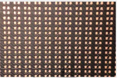
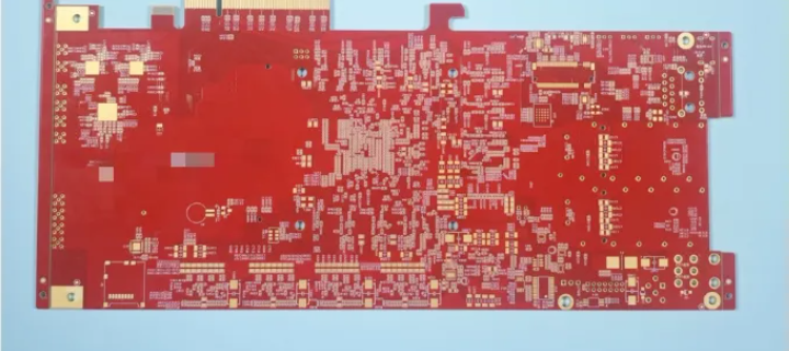
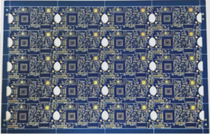
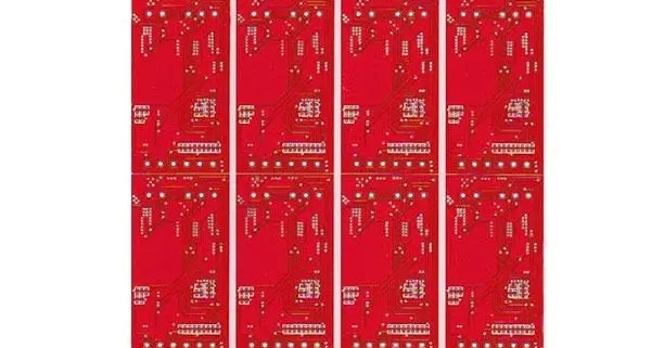
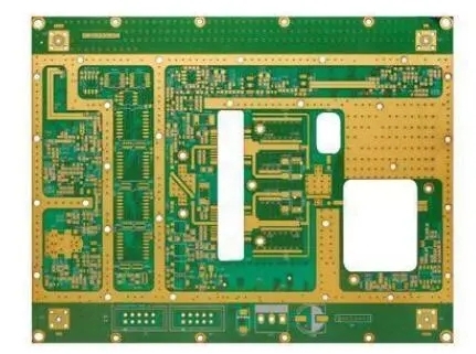
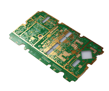
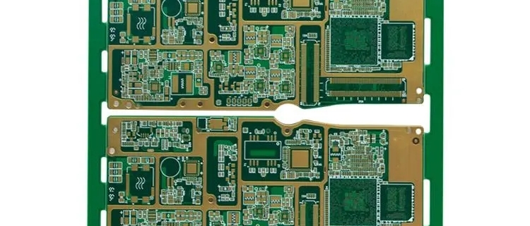
How to effectively deal with common quality problems of HDI circuit boards?

In the rapidly developing field of electronic manufacturing, high-density interconnect (HDI) circuit boards have become the core components of many electronic products due to their excellent performance and wide application. However, HDI circuit boards often encounter some quality problems during the manufacturing process. How to effectively deal with these problems is the key to improving product quality and ensuring market competitiveness.
Common quality problems and causes
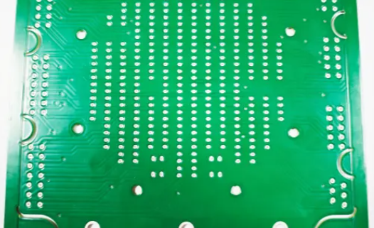
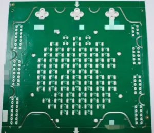
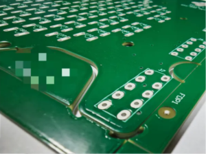
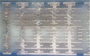
Circuit breakage and short circuit: Due to the high integration and precision design of HDI boards, the circuit spacing is small, and the slightest carelessness during processing may cause circuit breakage or short circuit.
Poor welding: Problems such as loose welding points, cold welding, etc. will seriously affect the electrical performance and reliability of HDI boards.
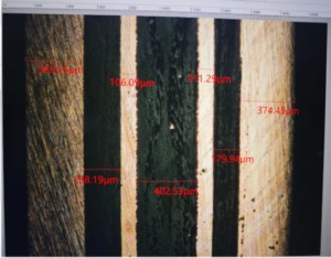
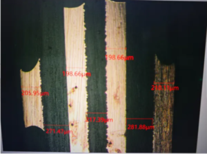
Material problems: The quality of materials such as substrate materials, copper foil, and solder mask ink is unstable, which will lead to the overall performance of HDI boards.
Improper process control: Improper control of key processes such as etching, drilling, and electroplating will also lead to quality problems.

Effective response strategies
Optimize design and process

Reasonable design: Fully consider the characteristics of HDI boards in the design stage, reasonably layout the circuits, and avoid overly compact designs.

Process optimization: According to the characteristics of HDI boards, optimize key processes such as etching, drilling, and electroplating to ensure processing accuracy and stability.
Strict material screening and control
Supplier selection: Select suppliers with credibility and quality assurance to ensure the quality of raw materials.

Material testing: Strictly test the raw materials entering the factory to ensure compliance with standards.
Strengthen process control and quality testing

Process monitoring: Establish a complete process control system to monitor and record key processes in real time.

Quality testing: Introduce advanced testing equipment to conduct comprehensive and detailed quality testing of hdi boards.
Improve employee skills and awareness

Skill training: Strengthen employee skills training to improve employees’ understanding and response capabilities to hdi board quality issues.

Quality awareness: Improve employees’ quality awareness so that every employee understands the importance of quality.
Establish a quality management system

System establishment: Establish a complete quality management system, from design, raw materials, production to testing, each link has clear standards and processes.

Continuous improvement: Through regular quality reviews and internal audits, problems are discovered and continuously improved.
The response to hdi circuit board quality issues requires us to start from multiple aspects, including optimizing design and process, strict material screening and control, strengthening process control and quality testing, improving employee skills and awareness, and establishing a quality management system. Only in this way can we ensure that the quality of hdi circuit boards is stable and reliable and meet market demand.

What are the PCB board materials?

Introduction to PCB circuit board materials:

The classification from bottom to top is as follows:

94HB/94VO/22F/CEM-1/CEM-3/FR-4

The details are as follows:

94HB: Ordinary cardboard, not fireproof (the lowest grade material, die-punched, cannot be used as a power board)

94V0: Flame retardant cardboard (die punching)

22F: Single-sided semi-fiberglass board (die punching)

CEM-1: Single-sided fiberglass board (must be computer drilled, not punched)

CEM-3: Double-sided semi-glass fiber board (except for double-sided cardboard, it is the lowest-end material for double-sided panels. Simple double-sided panels can use this material, which is 5~10 yuan/square meter cheaper than FR-4)

FR-4: Double-sided fiberglass board

Best answer

1.c The classification of flame retardant properties can be divided into four types: 94V-0/V-1/V-2 and 94-HB

2. Pre-cured sheet: 1080=0.0712mm, 2116=0.1143mm, 7628=0.1778mm

3. FR4 CEM-3 both represent boards, fr4 is fiberglass board, and cem3 is composite substrate

4. Halogen-free refers to substrates that do not contain halogens (fluorine, bromine, iodine and other elements), because bromine will produce toxic gases when burned, which is environmentally friendly.

6. Tg is the glass transition temperature, that is, the melting point.

Circuit boards must be flame-resistant and cannot burn at a certain temperature, only softening. The temperature point at this time is called the glass transition temperature (Tg point). This value is related to the dimensional stability of the PCB board.

What is a high Tg PCB circuit board and the advantages of using high Tg PCB

When the temperature of a high-Tg printed board rises to a certain area, the substrate will change from “glass state” to “rubber state”. The temperature at this time is called the glass transition temperature (Tg) of the board. In other words, Tg is the maximum temperature (°C) at which the substrate remains rigid. That is to say, ordinary PCB substrate materials not only soften, deform, melt, etc. under high temperatures, but also show a sharp decline in mechanical and electrical properties (I think you don’t want to see this happen to your products).

Generally, the Tg of the plate is above 130 degrees, the high Tg is generally above 170 degrees, and the medium Tg is about above 150 degrees.

Usually PCB printed boards with Tg≥170℃ are called high Tg printed boards.

As the Tg of the substrate increases, the heat resistance, moisture resistance, chemical resistance, stability resistance and other characteristics of the printed board will be increased and improved. The higher the TG value, the better the temperature resistance of the plate. Especially in the lead-free process, there are many high Tg applications.

High Tg refers to high heat resistance. With the rapid development of the electronics industry, especially electronic products represented by computers, which are developing towards high functionality and high multi-layering, higher heat resistance of PCB substrate materials is required as an important guarantee. The emergence and development of high-density mounting technologies represented by SMT and CMT have made PCBs increasingly inseparable from the support of high heat resistance of the substrate in terms of small apertures, fine wiring, and thinness.

Therefore, the difference between general FR-4 and high Tg FR-4 is: in the hot state, especially when heated after absorbing moisture, the material’s mechanical strength, dimensional stability, adhesion, water absorption, and thermal decomposition properties There are differences in various conditions such as thermal expansion and thermal expansion. High Tg products are obviously better than ordinary PCB substrate materials.

In recent years, the number of customers requesting the production of high-Tg printed boards has increased year by year.

PCB board knowledge and standards (2007/05/06 17:15)

At present, the following types of copper-clad laminates are widely used in our country. Their characteristics are shown in the table below: Types of copper-clad laminates, knowledge of copper-clad laminates

There are many ways to classify copper clad laminates. Generally, according to the different reinforcing materials of the board, it can be divided into: paper base, glass fiber cloth base,

There are five categories: composite base (CEM series), laminated multi-layer board base and special material base (ceramic, metal core base, etc.). If the panel is used

The resin adhesives are classified differently, the common paper-based CCI. There are: phenolic resin (XPc, XxxPC, FR-1, FR

-2 etc.), epoxy resin (FE-3), polyester resin and other types. Common fiberglass cloth-based CCLs include epoxy resin (FR-4, FR-5), which is currently the most widely used fiberglass cloth-based type. There are also other special resins (using glass fiber cloth, polyamide fiber, non-woven fabric, etc. as additional materials): bismaleimide-modified triazine resin (BT), polyimide resin (PI) , diphenylene ether resin (PPO), maleic anhydride imine-styrene resin (MS), polycyanate resin, polyolefin resin, etc. According to the flame retardant performance of CCL, it can be divided into two types of boards: flame retardant type (UL94-VO, UL94-V1 level) and non-flame retardant type (UL94-HB level). In the past year or two, as more attention has been paid to environmental protection issues, a new type of CCL that does not contain bromine has been divided into flame-retardant CCL, which can be called “green flame-retardant CCL”. With the rapid development of electronic product technology, there are higher performance requirements for cCL. Therefore, from the performance classification of CCL, it is divided into general performance CCL, low dielectric constant CCL, high heat resistance CCL (generally the L of the board is above 150°C), and low thermal expansion coefficient CCL (generally used on packaging substrates). ) and other types. With the development and continuous progress of electronic technology, new requirements are constantly put forward for printed board substrate materials, thus promoting the continuous development of copper-clad laminate standards. Currently, the main standards for substrate materials are as follows.

①National standards At present, my country’s national standards for substrate materials include GB/T4721-47221992 and GB4723-4725-1992. The copper-clad laminate standard in Taiwan is the CNS standard, which was formulated based on the Japanese JIs standard in 1983. Released in year.

Please do not copy the content of this site

②The main standards of other national standards include: Japan’s JIS standard, American ASTM, NEMA, MIL, IPC, ANSI, UL standards, British Bs standard, German DIN and VDE standards, French NFC and UTE standards, and Canadian CSA Standards, Australian AS standards, former Soviet Union FOCT standards, international IEC standards, etc.

Suppliers of original PCB design materials, some of which are commonly seen by everyone, include: Shengyi\Jiantao\International, etc.

● Accepted files: protel autocad powerpcb orcad gerber or real board copying, etc.

●Plate type: CEM-1, CEM-3 FR4, high TG material;

● Maximum board size: 600mm*700mm (24000mil*27500mil)

● Processing board thickness: 0.4mm-4.0mm (15.75mil-157.5mil)

●Maximum number of processing layers: 16Layers

●Copper foil layer thickness: 0.5-4.0(oz)

● Finished plate thickness tolerance: +/-0.1mm (4mil)

● Molding dimensional tolerance: Computer milling: 0.15mm (6mil) Mold punching: 0.10mm (4mil)

● Minimum line width/space: 0.1mm (4mil) Line width control capability: <+-20% ● Minimum drilling hole diameter of finished product: 0.25mm (10mil) Minimum punching hole diameter of finished product: 0.9mm (35mil) Finished product aperture tolerance: PTH: +-0.075mm (3mil) NPTH: +-0.05mm(2mil) ● Finished hole wall copper thickness: 18-25um (0.71-0.99mil) ● Minimum SMT patch spacing: 0.15mm (6mil) ●Surface coating: chemical immersion gold, spray tin, whole plate nickel gold plating (water/soft gold), screen printing blue glue, etc. ● Solder mask thickness on the board: 10-30μm (0.4-1.2mil) ● Peel strength: 1.5N/mm (59N/mil) ● Solder mask hardness: >5H

● Solder mask hole capability: 0.3-0.8mm (12mil-30mil)

● Dielectric constant: ε= 2.1-10.0

● Insulation resistance: 10KΩ-20MΩ

●Characteristic impedance: 60 ohm±10%

● Thermal shock: 288℃, 10 sec

● Warpage of finished board: <0.7%

● Product applications: communication equipment, automotive electronics, instrumentation, global positioning systems, computers, MP4, power supplies, home appliances, etc.

The role of using three proof paint in PCBA processing.

As one of the key links in the electronic product manufacturing industry, PCBA processing has an importance that cannot be ignored in the modern industrial field. In the PCBA processing process, the use of conformal anti-paint with its unique characteristics can not only effectively protect the circuit board from damage caused by water immersion, pollution and other factors, but also improve the reliability and stability of electronic products. . Next, we will delve into the role of conformal paint in PCBA processing and introduce in detail its importance in protecting circuit boards from water, dust and corrosion.

1. Protect the circuit board from water

Water resistance is a crucial consideration in the manufacturing process of electronic products. Since the circuit board contains many precision electronic components, the penetration of moisture will cause short circuits, insulation failure and other problems on the circuit board, which will seriously affect the normal operation of the product. The conformal anti-paint used in PCBA processing was introduced to solve this problem. The conformal anti-paint has good waterproof performance and can effectively isolate the erosion of external moisture and protect the circuit board from the threat of moisture.

2. Protect circuit boards from dust

In addition to waterproofing, dustproofing is also an important aspect to consider during PCBA processing. The tiny size and high sensitivity of electronic components make them extremely susceptible to contamination by dust and impurities. These contaminants can affect the normal operation of the circuit board and even cause circuit short circuits. Therefore, the use of conformal paint during PCBA processing can effectively isolate the circuit board from dust and protect the normal operation of electronic components.

3. Protect circuit boards from corrosion

In addition to being waterproof and dustproof, the conformal paint used in PCBA processing also has anti-corrosion functions. During the manufacturing and use of electronic products, circuit boards are easily susceptible to corrosion and failure due to the presence of oxygen, moisture, chemicals and other factors. The use of conformal paint can provide a protective film for circuit boards, effectively isolate external corrosion factors and extend the service life of electronic products.

In summary, the use of conformal paint in PCBA processing plays an irreplaceable and important role in protecting circuit boards from water, dust and corrosion. By using conformal coating, it can not only enhance the water, dust and corrosion resistance of electronic products and extend their service life, but also improve the reliability and stability of the product. Therefore, in the PCBA processing process, the rational use of conformal paint is a necessary means to ensure the quality and performance of electronic products.

How to check the quality of PCB circuit board after laser welding?

As 5G construction continues to advance, industrial fields such as precision microelectronics and aviation and shipbuilding have further developed, and these fields all cover the application of PCB circuit boards. With the continuous development of these microelectronics industries, we will find that the manufacturing of electronic components is gradually becoming miniaturized and thinner, and the requirements for precision are getting higher and higher. As the most commonly used processing technology in the microelectronics industry, laser welding is bound to There are increasingly higher requirements for the welding level of PCB circuit boards.

Inspection after PCB circuit board welding is very important for both enterprises and customers. In particular, many enterprises have strict requirements for electronic products. If inspection is not done, performance failures will easily occur, affecting product sales, corporate image and word of mouth. The laser welding equipment produced by Shenzhen Zichen Laser has fast efficiency, high welding yield, and post-weld inspection function, which can meet the welding processing and post-weld inspection needs of enterprises. So, how to check the quality of PCB circuit board after welding? Below Zichen Laser shares several commonly used detection methods.

01 PCB triangulation

What is triangulation? That is, the method used to check the three-dimensional shape. At present, the triangulation detection method has been developed and used and equipment capable of detecting its cross-sectional shape has been designed. However, because this triangulation detection method is incident from different lights and in different directions, the observation results will be different. Essentially, objects are inspected through the principle of light diffusion. This method is the most appropriate and most effective. As for the situation where the welding surface is close to mirror surface conditions, this method is inappropriate and difficult to meet production needs.

02 Light reflection distribution measurement method

This method mainly uses the welding part to detect the decoration, injects light inward from an oblique direction, sets a TV camera above, and then inspects it. The most important part of this operation method is how to know the surface angle of the PCB solder, especially how to know the irradiation photometric information. The angle information must be captured through various light colors. On the contrary, if it is illuminated from above, the angle measured is the reflected light distribution, and just check the tilted surface of the solder.

03 Change the angle for camera inspection

How to detect PCB after welding? To use this method to detect the quality of PCB after welding, a device with a changing angle is necessary. This device generally has at least 5 cameras, multiple LED lighting equipment, uses multiple images, and uses visual inspection conditions for inspection, so the reliability is relatively high.

04 Focus detection utilization method

For some high-density circuit boards, after PCB welding, the above three methods are difficult to detect the final result, so the fourth method, which is the focus detection and utilization method, needs to be used. This method is divided into multiple methods, such as the multi-stage focus method, which can directly detect the height of the solder surface and achieve high-precision detection. If 10 focus surface detectors are set up at the same time, the focus surface can be obtained by seeking the maximum output and detect The position of the solder surface. If it is detected by irradiating the object with a fine laser beam, a lead device with a pitch of 0.3mm can be successfully detected by staggering 10 specific pinholes in the Z direction.

BGA welding working principle, solder joint inspection and rework procedures.

Ball grid array (BGA) packaging has become one of the most popular technologies for integrated circuits requiring high input/output counts. BGA packaging has advantages over other methods due to its high-density interconnect capabilities. As integrated circuit complexity increases, and pin and gate counts continue to grow, BGAs become the optimal packaging solution to balance cost and performance. In this guide, we’ll explain BGA soldering – the process of attaching a BGA package to a printed circuit board. We’ll cover how BGA soldering works, solder joint inspection, and rework procedures. By understanding the ball grid array soldering process, its challenges and solutions, manufacturers can effectively leverage this advanced packaging technology.

What is BGA

BGA is a unique surface mount package used to secure and mount SMD electronic components to integrated circuits on the surface of SMT printed circuit boards. BGAs have ball leads that are distributed in an array on the bottom of the package. And the ball array actually gets its name because it is an array of metal or alloy balls arranged in a grid.

BGA package is used to permanently mount the device. It provides more interconnect pins where you can place a flat or dual in-line package. The pins used in this technology are solder balls that are arranged in a pattern, usually a grid-like pattern, on the lower surface of the package. This is done to increase the connection area, not just the periphery. The most interesting thing is that with BGA soldering you have the benefit of using the entire underside of the device rather than just the perimeter.

This technology is used in various electronic products to install different integrated circuits such as FPGAs, WiFi chips, FPGAs, etc. What’s more, these packages are also used in RAM devices, PC chipsets, and microcontrollers.

How BGA soldering works

First, apply solder paste to the PCB pads that the BGA solder balls will contact. Solder paste is typically dispensed via a stencil or screen printing process to ensure accurate and repeatable application.

The BGA components are then precisely positioned and temporarily affixed to the PCB. This is accomplished using pick-and-place equipment with high-precision XY motion control and optical alignment systems. Proper alignment is critical.

PCB A is then fed into a reflow oven with a prescribed temperature profile. The solder paste melts, and the BGA’s solder balls melt and fuse with the PCB pads, forming solder joints. The profile must be hot enough to reflow the solder without damaging the components.

Finally, after cooling, check that the solder joints are formed correctly and have no defects. Any required rework is completed using specialized BGA rework equipment and procedures.

BGA solder joint inspection

When BGA packages were first introduced, there was uncertainty about how to verify solder joints because they were not visible underneath the component. Traditional optical inspection methods cannot be used. Additionally, electrical tests lack reliability because they only reflect the conductivity of the BGA at a specific moment of testing. This method cannot predict the long-term durability of the solder and may cause the solder joint to fail over time.

In order to truly inspect BGA solder joints, X-ray imaging technology is required. X-rays can penetrate components and capture images of hidden joints. Therefore, X-ray inspection is critical for process control and quality assurance when assembling circuit boards using BGAs. X-ray inspection provides the needed confidence by verifying that all joints are formed completely correctly. With X-rays, manufacturers can verify their BGA processes and ensure the long-term reliability required for these hidden interconnects.

BGA rework

When a BGA component is found to be defective, a rework process is required to remove and replace it. Solder joints must be carefully melted without disturbing adjacent components. This is achieved through a BGA rework station that utilizes targeted heat and airflow.

Infrared preheaters gently heat the circuit board from below to minimize thermal shock. Thermocouples monitor temperature in real time. After reflow, the vacuum tool lifts the BGA package. Strict process control is critical to success:

Match solder alloys to ensure joint compatibility

Balance bond strength for positioning adjustments

Strictly adhere to prescribed thermal curves

Use the minimum airflow setting required

Raise BGA slowly after reflow to avoid scrubbing

Choose a nozzle size that matches the component

With experience and rigorous procedures, reworked BGAs can become reliable. But it requires great precision and care to avoid collateral damage. Carefully tuned processes, specialized tools and operator skills are key drivers of high-quality BGA rework results.

final thoughts

Implementing a robust BGA soldering, inspection, and rework process requires investments in technical expertise, equipment, and operator training. But the advantages of higher-density BGA packaging make the effort worthwhile in terms of quality and performance. With expertise in precision printing, accurate placement, profile reflow, X-ray inspection and controlled rework, manufacturers like MOKO Technology enable customers to get the most out of BGAs in critical applications. As a leading PCB assembly supplier with nearly 20 years of experience, MOKO focuses on advanced ball grid array soldering technology. Please contact us today to discuss your specific BGA project and assembly requirements.

Analysis of the causes of lack of copper in half holes of PCB boards and their effects!

In the electronics manufacturing industry, PCB (Printed Circuit Board) board serves as a “neural network” connecting electronic components, and its quality directly affects the performance and stability of the entire electronic device. As a common manufacturing problem, half-hole copper deficiency in PCB boards has complex causes and far-reaching consequences. This article will deeply analyze the reasons for the lack of copper in the half-hole of the PCB board and discuss its possible impact.
1. Analysis of the causes of lack of copper in half holes of PCB boards
Drilling process issues
Insufficient precision of drilling equipment: Low-precision drilling equipment may result in inconsistent hole sizes, rough or damaged hole walls.
Drill bit selection and wear: Unsuitable drill bits or excessively worn drill bits will affect the quality of drilling.
Improper drilling parameter settings: Unreasonable settings such as feed speed, rotation speed, etc. will also cause damage to the hole wall.

Electroplating copper process issues
Electroplating solution composition and concentration: The copper ion concentration in the electroplating solution is too low or too high, which may affect the electroplating effect.
Electroplating solution temperature and pH value: Improper temperature or pH value will affect the adhesion and uniformity of the electroplated copper layer.
Current density and time: The current density is too high or too small, and the plating time is too short or too long, which will lead to poor copper layer quality.

plate problem
Uneven material of the board: There are impurities or inconsistent fiber directions inside the board, which will affect the adhesion and uniformity of the electroplated copper layer.
Improper plate pretreatment: If the pretreatment process such as oil removal and rust removal is not in place, it will affect the subsequent electroplating effect.

Operational and Management Issues
Insufficient operator skills: The skill level of operators directly affects product quality.
Strict quality inspection: Strict quality inspection of semi-finished products and finished products may cause problematic products to flow into the next process.

2. The impact of lack of copper in the half hole of PCB board
Reduced electrical performance: Lack of copper in half holes can lead to poor circuit connections, increase resistance, and reduce the electrical performance of electronic devices.

Reduced equipment stability: Poor circuit connections may cause short circuits, open circuits and other faults during operation of the equipment, reducing the stability and reliability of the equipment.

Increased production costs: The lack of copper in half holes will increase the scrap rate and repair rate of products, leading to an increase in production costs. At the same time, more time and resources may need to be invested in technical improvements and quality control to solve this problem.

Damage to market competitiveness: PCB board quality issues are an important factor affecting a company’s brand image and reputation. If the product has quality problems such as half-hole copper shortage, it will affect customers’ trust in the company and reduce market competitiveness.
3. Solution Strategies and Suggestions
Improve equipment and process level: introduce advanced drilling equipment and electroplating equipment, optimize process parameter settings, and ensure the stability and reliability of the drilling and electroplating process.

Strictly screen and inspect boards: Strictly screen and inspect the base materials of PCB boards to ensure that the quality of the boards meets the requirements. At the same time, the pretreatment process control of the plate is strengthened to ensure that the hole wall is clean and free of impurities.

Strengthen operation and management training: improve the skill level of operators and strengthen the rigor of quality inspection. Establish a complete quality traceability system to promptly trace and analyze problematic products.

Adopt new technologies and new materials: Explore the use of new technologies and new materials to improve the manufacturing quality and performance of PCB boards. For example, advanced technologies such as laser drilling technology and nano-plating technology are used to improve product accuracy and reliability.
The lack of copper in the half hole of the PCB board is a problem that needs attention. By in-depth analysis of its causes and adopting effective solution strategies, we can reduce the incidence of half-hole copper shortage problems, improve the quality and performance of PCB boards, and thereby enhance the market competitiveness of enterprises.

Discussion on PCB ink plugging process: How to ensure the stability and reliability of the circuit board!

In electronics manufacturing, the stability and reliability of PCBs (Printed Circuit Boards) are crucial. The PCB ink hole plugging process is one of the key steps to ensure circuit board performance. It involves using special ink to fill conductive holes to prevent short circuits between different layers. This article will delve into the PCB ink plugging process and share how to ensure the stability and reliability of the circuit board through this process.
1. The importance of PCB ink plug holes
Prevent short circuit: Different conductive layers can be effectively isolated through plug holes to avoid short circuit caused by current leakage.

Ensure signal integrity: Good hole plugging technology can reduce interference during signal transmission and maintain signal clarity and stability.

Improved mechanical strength: The circuit board after plugging the holes can better withstand physical stress and improve the overall mechanical stability.
2. Key measures to ensure stability and reliability
Choose the right ink: Depending on the application needs of the circuit board, choose an ink with good electrical insulation, high adhesion, and good chemical resistance.

Precisely control the plugging process: Strictly control the temperature, pressure and time during the plugging process to ensure that the ink is fully filled and solidified.

Use high-quality equipment: Use high-precision plugging equipment to improve the quality and efficiency of plugging.

Implement strict quality inspection: comprehensively inspect the plugging effect through methods such as automatic optical inspection (AOI) and X-ray inspection.
3. Strategies for optimizing hole plugging process
Optimize design layout: Consider the need for hole plugging during the design stage to avoid an overly dense hole layout and ensure that the ink can be fully filled.

Conduct material compatibility testing: Conduct compatibility testing on inks and sheets before production to ensure that their interaction meets requirements.

Regularly maintain equipment: Regularly maintain and calibrate plughole equipment to maintain optimal performance.

Continuous process improvement: Based on production feedback and reliability test results, the hole plugging process is continuously optimized to improve the quality of the circuit board.
PCB ink plugging process is a key link to ensure the stability and reliability of the circuit board. By choosing the right inks, precisely controlling the hole plugging process, using high-quality equipment, and implementing strict quality inspections, manufacturers can effectively improve the performance of their circuit boards. At the same time, optimizing design layout, conducting material compatibility testing, regular maintenance of equipment and continuous improvement of processes will further ensure the long-term stability and reliability of circuit boards. With the continuous advancement of electronic technology, the requirements for PCB manufacturing are becoming higher and higher, which requires manufacturers to continuously innovate and improve plug hole technology to meet the challenges of the future electronics industry.

Cost and performance trade-off of 4-layer PCB board!

With the rapid development of science and technology, electronic products have become increasingly popular. As the core component of electronic products, the importance of PCB boards (printed circuit boards) is self-evident. Among the many PCB board types, 4-layer PCB boards have attracted much attention due to their excellent performance and wide range of application fields.
Price factors of customized 4-layer PCB board
The price of customized 4-layer PCB boards is affected by many factors, including the following aspects:
Plate selection: The prices of plates of different materials and thicknesses vary greatly. Generally speaking, high-performance boards are more expensive but offer better electrical performance and mechanical strength.

Design complexity: The higher the design complexity, the more difficult the processing and the cost will increase accordingly. For example, PCB boards that require more process steps such as drilling and milling will be more expensive.

Production batch: The larger the production batch, the lower the single-chip cost. Because in mass production, equipment and human resources can be fully utilized to reduce unit costs.

Delivery time: If the customer has strict requirements on delivery time, additional expedited fees may be required.
Cost and performance trade-offs for 4-layer PCB boards
When choosing a custom 4-layer PCB board, we need to make a trade-off between cost and performance. Here are some factors worth considering:
Performance requirements: We need to clarify the performance requirements of the product. If the product has higher requirements on electrical performance, stability, reliability, etc., then we should choose higher performance boards and more sophisticated design solutions, but this may increase the cost.

Budget constraints: After clarifying the performance requirements, we need to consider budget constraints. If the budget is limited, we need to reduce costs as much as possible while meeting performance requirements. This may require us to make compromises in plate selection, design complexity, etc.

Delivery Time: Delivery time is also a factor to consider. If customers have strict requirements on delivery time, we may need to choose faster production processes and more expensive plates to ensure on-time delivery. But it can also increase costs.
The price of customized 4-layer PCB boards is affected by many factors, including board selection, design complexity, production batch size, and delivery time. When choosing a custom 4-layer PCB board, we need to make a trade-off between cost and performance to meet the product’s performance needs and budget constraints. By referring to the price list and considering various factors, we can choose the customized 4-layer PCB board that best suits our needs.

10 PCB cooling tips to help you improve.

For electronic equipment, a certain amount of heat will be generated during operation, causing the internal temperature of the equipment to rise rapidly. If the heat is not dissipated in time, the equipment will continue to heat up, and the device will fail due to overheating. The reliability of electronic equipment Performance will decrease.
Therefore, it is very important to handle the heat dissipation of the circuit board well. The heat dissipation of PCB circuit board is a very important link. So what are the heat dissipation techniques of PCB circuit board? Let’s discuss it together.

01

Heat dissipation through the PCB board itself. The currently widely used PCB boards are copper-clad/epoxy glass cloth base materials or phenolic resin glass cloth base materials, and there are also a small amount of paper-based copper-clad sheets.
Although these substrates have excellent electrical properties and processing properties, they have poor heat dissipation. As a heat dissipation path for high-heating components, it is almost impossible to expect the PCB resin itself to conduct heat, but to dissipate heat from the surface of the component to the surrounding air.
However, as electronic products have entered the era of component miniaturization, high-density installation, and high-heat assembly, it is not enough to rely solely on the surface of components with very small surface areas to dissipate heat.
At the same time, due to the extensive use of surface-mounted components such as QFP and BGA, the heat generated by the components is transferred to the PCB board in large quantities. Therefore, the best way to solve the problem of heat dissipation is to improve the heat dissipation capacity of the PCB itself that is in direct contact with the heating components, through the PCB board Conduct or radiate out.

▼Add heat dissipation copper foil and use large-area power supply ground copper foil
图片
▼Thermal vias
图片
▼The copper is exposed on the back of the IC to reduce the thermal resistance between the copper and the air
图片

PCB layout
Heat-sensitive devices are placed in the cold air area.
The temperature detection device is placed in the hottest location.
Devices on the same printed board should be arranged according to their heat generation and heat dissipation degree as much as possible. Devices with small heat generation or poor heat resistance (such as small signal transistors, small-scale integrated circuits, electrolytic capacitors, etc.) should be placed in the cooling air flow. At the top of the cooling air flow (at the entrance), devices with high heat generation or good heat resistance (such as power transistors, large-scale integrated circuits, etc.) are placed at the bottom of the cooling air flow.
In the horizontal direction, high-power devices should be placed as close to the edge of the printed board as possible to shorten the heat transfer path; in the vertical direction, high-power devices should be placed as close to the top of the printed board as possible to reduce the impact of these devices on the temperature of other devices when they are working. .
The heat dissipation of printed boards in equipment mainly relies on air flow, so the air flow path must be studied during design and the devices or printed circuit boards should be reasonably configured.
When air flows, it always tends to flow in places with low resistance, so when configuring devices on a printed circuit board, avoid leaving a large air space in a certain area. The same issue should also be paid attention to in the configuration of multiple printed circuit boards in the whole machine.
Devices that are more sensitive to temperature are best placed in the area with the lowest temperature (such as the bottom of the device). Never place it directly above the heating device. It is best to arrange multiple devices staggered on the horizontal plane.
Place the devices that consume the most power and generate the most heat near the best locations for heat dissipation. Do not place high-heat components in the corners and edges of the printed board unless a heat sink is arranged nearby.
When designing the power resistor, choose a larger device as much as possible, and make sure there is enough space for heat dissipation when adjusting the printed board layout.

Component spacing recommendations:
图片
02

Add radiators and heat conduction plates to high-heating devices. When there are a few devices in the PCB that generate a large amount of heat (less than 3), you can add radiators or heat pipes to the heating devices. When the temperature cannot be lowered, you can use Radiator with fan to enhance cooling effect.
When there are a large number of heating devices (more than 3), a large heat dissipation cover (board) can be used. It is a special radiator customized according to the position and height of the heating device on the PCB board or placed on a large flat-panel radiator. Cut out the high and low positions of different components. Attach the heat dissipation cover to the component surface and make contact with each component to dissipate heat.
However, due to the poor consistency of the components during assembly and soldering, the heat dissipation effect is not good. Usually, a soft thermal phase change thermal pad is added to the component surface to improve the heat dissipation effect.
图片

03

For equipment that uses free convection air cooling, it is best to arrange the integrated circuits (or other devices) vertically or horizontally.

04

Use reasonable wiring design to achieve heat dissipation. Since the resin in the board has poor thermal conductivity, and copper foil lines and holes are good conductors of heat, increasing the remaining rate of copper foil and adding thermal holes are the main means of heat dissipation. To evaluate the heat dissipation capability of PCB, it is necessary to calculate the equivalent thermal conductivity (nine eq) of the insulating substrate for PCB, which is a composite material composed of various materials with different thermal conductivity.

05

Devices on the same printed board should be arranged according to their heat generation and heat dissipation degree as much as possible. Devices with small heat generation or poor heat resistance (such as small signal transistors, small-scale integrated circuits, electrolytic capacitors, etc.) should be placed in the cooling air flow. At the top of the cooling air flow (at the entrance), devices with high heat generation or good heat resistance (such as power transistors, large-scale integrated circuits, etc.) are placed at the bottom of the cooling air flow.

06

In the horizontal direction, high-power devices should be placed as close to the edge of the printed board as possible to shorten the heat transfer path; in the vertical direction, high-power devices should be placed as close to the top of the printed board as possible to reduce the impact of these devices on the temperature of other devices when they are working. .

07

The heat dissipation of printed boards in equipment mainly relies on air flow, so the air flow path must be studied during design and the devices or printed circuit boards should be reasonably configured.
When air flows, it always tends to flow in places with low resistance, so when configuring devices on a printed circuit board, avoid leaving a large air space in a certain area.
The same issue should also be paid attention to in the configuration of multiple printed circuit boards in the whole machine.

08

Devices that are more sensitive to temperature are best placed in the area with the lowest temperature (such as the bottom of the device). Never place it directly above the heating device. It is best to arrange multiple devices staggered on the horizontal plane.

09

Place the devices that consume the most power and generate the most heat near the best locations for heat dissipation. Do not place high-heat components in the corners and edges of the printed board unless a heat sink is arranged nearby. When designing the power resistor, choose a larger device as much as possible, and make sure there is enough space for heat dissipation when adjusting the printed board layout.

10

Avoid the concentration of hot spots on the PCB, distribute the power evenly on the PCB as much as possible, and keep the PCB surface temperature performance uniform and consistent.
It is often difficult to achieve strict uniform distribution during the design process, but areas with too high power density must be avoided to avoid hot spots that may affect the normal operation of the entire circuit.
If possible, it is necessary to conduct thermal efficiency analysis of printed circuits. For example, the thermal efficiency index analysis software module added to some professional PCB design software can help designers optimize circuit design.