How to solve the material compatibility problem in SMT patch processing?

The key to solving the material compatibility problem in SMT patch processing is to ensure that all materials used can remain stable during the processing and will not produce adverse reactions with each other. The specific analysis is as follows:

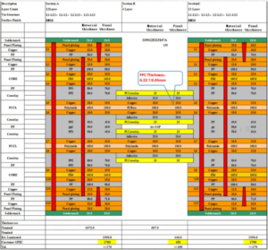
1. Choose the right solder paste. Solder paste matching: Select the right solder paste according to the heat capacity and welding temperature of the PCB board and components. Solder paste composition analysis: Ensure that the components in the solder paste are compatible with the metal plating of the PCB board and components to avoid adverse reactions.

2. Evaluate the heat resistance of the substrate material. Select a substrate material that can withstand the high temperature during the SMT patch processing to prevent the substrate from being deformed or damaged. Surface treatment suitability: Consider the substrate surface treatment process, such as tin spraying, OSP (organic protective agent), silver, etc., to ensure a good welding effect.

3. Consider the compatibility of component materials and component packaging materials: Check whether the packaging materials of the components can adapt to the automated production line of the SMT machine to avoid reduced production efficiency due to material incompatibility. Component heat resistance: Ensure that all components can withstand the high temperature during SMT patch processing to prevent component damage.

4. Optimize the process temperature curve optimization: adjust the temperature curve of reflow soldering according to the characteristics of different materials to ensure the quality of welding while avoiding material damage. Process control: implement strict process control, including the management of temperature and humidity in the production environment to reduce the instability of materials caused by environmental changes.

5. Conduct tests to verify compatibility tests: conduct small batch compatibility tests before formal production to verify the compatibility between different materials. Reliability testing: conduct comprehensive reliability tests on samples that have completed SMT patch processing, including but not limited to temperature cycle tests, mechanical impact tests, etc., to ensure long-term stability.

To solve the material compatibility problem in SMT patch processing, it is necessary to start from multiple angles and comprehensively consider the physical and chemical properties of various materials, which can effectively reduce the risks caused by material incompatibility and improve production efficiency and PCBA product quality.

What are the application cases of wireless charger circuit boards in different industries?

The application cases of wireless charger circuit boards in different industries are very extensive, covering multiple fields such as consumer electronics, automotive electronics, smart home, medical equipment and industrial applications. The following are some specific application cases:

Consumer electronics industry

1. Smartphones and tablets: Smartphones and tablets are one of the most common applications of wireless charger circuit boards. Users only need to place their mobile phones or tablets on the wireless charging pad to achieve a cable-free charging experience. This convenience makes wireless charging very popular in the consumer market.

2. Wearable devices: Wearable devices such as smart watches and wireless headphones also support wireless charging. These devices usually have a small battery capacity but a high frequency of use. The convenience of wireless charging is of great significance to improving user experience.

Automotive electronics industry

1. Wireless charging of electric vehicles: Wireless charging technology for electric vehicles is gradually maturing and commercializing. The wireless charging system is divided into a transmitter (installed on the ground or parking space) and a receiver (installed at the bottom of the electric vehicle). When the electric vehicle is parked in the charging area, the wireless transmission of electrical energy is achieved through the principle of electromagnetic induction. This technology reduces physical contact during charging and improves the convenience and safety of charging.

2. Car wireless charger: Many car PCB manufacturers have integrated wireless chargers in the car to facilitate drivers and passengers to wirelessly charge mobile phones and other devices. This design not only enhances the sense of technology in the car, but also avoids the problem of cable clutter caused by traditional wired charging.

Smart home industry

1. Wireless charging of smart home devices: In the field of smart home, wireless charging technology is also widely used in various smart devices. For example, smart speakers, smart door locks and other devices can be charged through wireless charging plates without frequent battery replacement or plugging and unplugging charging cables.

2. Furniture integrated wireless charging: Some high-end furniture such as coffee tables and bedside tables also integrate wireless charging functions. Users only need to place mobile phones and other devices on furniture to charge. This design not only improves the practicality of furniture, but also increases the convenience of home life.

Medical equipment industry

1. Wireless charging of medical instruments: In the field of medical equipment, wireless charging technology is used to charge various portable medical instruments. For example, electrocardiographs, blood glucose meters and other devices can be charged through wireless charging plates, avoiding the risk of cross infection that may be caused by traditional wired charging.

2. Wireless charging of medical robots: Medical robots such as surgical robots and nursing robots also use wireless charging technology. This technology allows robots to perform tasks without frequently returning to charging stations for charging, improving work efficiency and safety.

Industrial applications

1. Wireless charging of industrial equipment: In the industrial field, wireless charging technology is used to charge various industrial equipment. For example, robots, drones and other equipment on automated production lines can be charged through wireless charging pads, reducing manual intervention and downtime.

2. Wireless charging of industrial environment monitoring equipment: Some industrial environment monitoring equipment such as temperature sensors and humidity sensors also use wireless charging technology. These devices are usually deployed in inaccessible or dangerous environments. Wireless charging technology eliminates the need for maintenance personnel to frequently enter these environments for charging operations.

There are many application cases of wireless charger circuit boards in different industries. With the continuous advancement of technology and the reduction of costs, wireless charging technology will be widely used and promoted in more fields.

12-layer Rigid-Flex HDI PCB

The development of PCB can be traced back to the 1950s, when it started with the quantitative production of some single-sided and double-sided PCBs. In the 1970s, multi-layer PCBs developed rapidly, and continued to move towards high precision, high density, and high reliability. This also laid the foundation for the rigid-flex board. In the birth and continuous development of FPC and PCB, a new product, the rigid-flex board, was born. It can be said that the rigid-flex board is the youngest member of the PCB family.

Early Rigid-Flex PCBs were mainly used in military and aerospace fields that have extremely high requirements for reliability and performance, such as aircraft, missiles and other high-end equipment. Today  SHENZHEN BEST PCBA CO.,LIMITED bring you a 12-layer HDI Rigid-Flex PCB, let’s take a look at it first!

Rigid-flex boards can be said to be a beautiful work of art in PCB products! In the same level of rigid-flex boards, a variety of different stacking structures can be produced. For example, a 12-layer rigid-flex board can be a 10-layer rigid board + 2-layer flex board structure, or an 8-layer rigid board + 4-layer flex board structure, or a 6-layer rigid board + 6-layer flex board structure. The layer settings of soft and hard boards are not fixed, and can be set by engineers according to their needs! The internal structure of our 12-layer rigid-flex board is 8-layer rigid board + 4-layer flex board. Let’s appreciate its stacking structure:


L5-6, L7-8 are four-layer flex boards, and the other layers are FR4 rigid boards. In addition, this product is a 1 step blind and buried HDI. In order to ensure the stability and reliability of the product, we use  plugged with resin technology to fill the buried hole part, and the blind hole part is filled with electroplating.

Of course, this product is not used in general electronic equipment. It is a PCB for industrial control equipment!

We delivered the product perfectly to our customers!


How to understand the minimum rules for PCB line spacing and hole spacing?

With the trend of miniaturization and complexity of modern electronic devices, the accuracy and rationality of the design of PCB printed circuit boards as a connecting bridge between electronic components are particularly important. The design of PCB is not only related to the stable performance of the product, but also directly affects the manufacturing cost and production efficiency. Among the many design rules, the minimum setting of PCB line spacing (the distance between line widths) and hole spacing (the distance from the edge of the hole to the adjacent wire) is one of the key factors to ensure the normal operation of the circuit, avoid short circuits and improve the success rate of manufacturing.

Overview of PCB line spacing and hole spacing PCB line spacing refers to the minimum allowable distance between the center lines of any two conductive lines on the PCB. This distance must be large enough to prevent accidental electrical connections (i.e. short circuits) caused by damage to insulating materials during the manufacturing process or when the circuit is running. The size of the line spacing is affected by many factors such as the materials used, manufacturing process, operating voltage, expected current, and expected working environment.
Hole spacing refers to the minimum allowable distance from the edge of the hole (via used to install component pins or realize interlayer connection) on the PCB to the edge of the nearest wire. Reasonable hole spacing design can ensure that the drilling and copper plating process will not damage the adjacent wires, while reducing the crosstalk between signals and ensuring the signal integrity of the circuit.

Why is the minimum spacing rule established?

1. Electrical safety: Too small line spacing and hole spacing may cause current leakage, causing short circuits, and in severe cases, damage the circuit board or even the entire system.

2. Manufacturing feasibility: Different manufacturing processes have their technical limitations, such as etching accuracy, drilling accuracy, etc. Too small spacing will increase the difficulty of manufacturing and reduce the yield rate.

3. Signal integrity: Electromagnetic interference is easily generated between conductors that are too close, affecting the quality of signal transmission, causing signal attenuation, delay or distortion.

4. Thermal management: Dense layout may hinder heat dissipation and affect the long-term reliability and life of components.

Factors affecting the minimum spacing Circuit operating voltage and current: High voltage or high current circuits require larger line spacing to reduce the risk of breakdown. Signal frequency: High-frequency signals are more sensitive to line spacing to reduce crosstalk and ensure signal quality. Manufacturing process: Advanced manufacturing technology can support smaller line spacing and hole spacing, but the cost increases accordingly. Environmental factors: such as temperature cycling, humidity, etc., require more conservative designs to improve reliability in harsh environments.

Design practice recommendations Follow manufacturer guidelines: Each PCB manufacturer will provide specific manufacturing capability parameters, including minimum line spacing and hole spacing requirements, which must be strictly followed during design. Use design software assistance: Modern PCB design software usually has a built-in DRC (design rule check) function to help designers automatically detect and adjust line spacing and hole spacing that do not meet specifications. Reserve margin: Under the premise of meeting performance requirements, appropriately increase line spacing and hole spacing to leave room for manufacturing tolerances and potential design modifications. Multilayer board design considerations: For multilayer boards, it is also necessary to consider the impact of inter-layer alignment and via penetration on adjacent layers for comprehensive design.

In short, the line spacing and hole spacing of PCBs are one of the most basic and critical design elements, which are directly related to the performance, reliability and manufacturing cost of the circuit board. By deeply understanding these rules and combining specific project requirements and manufacturing capabilities, designers can effectively avoid common design errors and create electronic products that are both efficient and reliable.


How to optimize rail transit PCB to improve train operation stability and safety?

In order to optimize rail transit PCB to improve the stability and safety of train operation, the following aspects can be considered:

1. Improve the reliability and stability of PCB boards. Choose high-quality materials: Select PCB board materials with high reliability, long life and good heat resistance to ensure stable operation in harsh environments. Optimize manufacturing process: Through precise manufacturing process, reduce defects and defective rates in the manufacturing process and improve the overall quality of PCB boards. Redundant design: Redundant design is adopted in key components and signal transmission paths. Once a component fails, other components can take over the work to ensure continuous operation of the system.

2. Optimize the wiring design of PCB boards to reduce electromagnetic interference: Reasonably design the wiring to avoid cross interference and crosstalk between signal lines and reduce the impact of electromagnetic interference on system performance. Improve signal quality: Through reasonable wiring design, reduce signal attenuation and distortion, and improve the accuracy and reliability of signal transmission. Consider signal integrity: When transmitting high-speed signals, special attention should be paid to signal integrity issues, and appropriate topology and termination methods should be adopted to ensure signal quality.

3. Strengthen thermal management and arrange heat dissipation devices reasonably: Reasonably arrange heat dissipation devices such as heat sinks and heat pipes on PCB circuit boards to improve the conduction and dissipation efficiency of heat. Optimize the heat dissipation structure: Design a reasonable heat dissipation structure, such as increasing the heat dissipation area, using high-efficiency heat dissipation materials, etc., to ensure that the PCB board can work stably in a high temperature environment.

4.Enhance protection measures and select protective materials: Apply protective coatings or use protective materials on the surface of the PCB board to increase its ability to resist harsh environments, such as moisture-proof, dust-proof, and corrosion-proof. Conduct reliability tests: Conduct strict reliability tests during the design and manufacturing process to ensure that the PCB board can work normally under various harsh conditions.

5. Use intelligent technology to introduce intelligent monitoring: Integrate intelligent monitoring modules on the PCB board to monitor the operating status and parameters of the system in real time, and promptly discover and deal with potential problems. Intelligent scheduling and optimization: Combine big data and artificial intelligence technologies to intelligently schedule and optimize train operations to improve operating efficiency and safety.

6. Follow the fail-safe principle to design a fail-safe system: Follow the fail-safe principle in the design of the PCB board, that is, when a system or component fails, it can automatically switch to a safe state to prevent accidents. Strengthen fault detection and diagnosis: By improving fault detection and diagnosis capabilities, quickly and accurately locate the problem, and take appropriate measures to deal with it.

The above measures can significantly improve the performance and reliability of rail transit PCB boards, thereby ensuring the stability and safety of train operation.

Optical Chip Carrier PCB

As science and technology develop, people’s observation of things is getting deeper and deeper. The product we bring today is an optical chip carrier used in single-photon SPAD imaging detectors. SPAD plays an important role in many fields, including but not limited to astronomy, particle size determination, quantum computing, quantum key distribution, single molecule detection, etc.

Regarding SPAD, interested friends can check the relevant information. Today, we mainly introduce this optical chip carrier PCB.

The most difficult part of the product process is these two steps, which require two depth control gongs and laser lid opening, and the depth control requirements are very strict.

The surface treatment adopts the  ENEPIG process. The ENEPIG  has strong adhesion and is not easy to fall off, which improves the reliability and stability of the product.

In addition, as a carrier board, the circuit design of the product is high-precision and highly integrated. The line width and line spacing are designed to be only 2mil. The minimum binding pad is 0.070mm.

Although our product is only a 4-layer PCB, it needs to be pressed twice because of the steps. The following is the pressing structure diagram

PCB carrier is a special printed circuit board used to carry electronic components, with the characteristics of high precision, high reliability and high integration. It has excellent electrical, mechanical and thermal properties, and can meet the high performance requirements of various complex electronic systems. Its process is not as complicated as imagined, but the parameter requirements at the detail level are very strict!

How to perform signal integrity analysis on FPC impedance board?

Conducting signal integrity analysis of FPC (Flexible Printed Circuit) impedance board is a complex process involving multiple steps and techniques. Here are some basic steps and considerations:

1. Understand the characteristics of FPC impedance board: First, you need to have a deep understanding of the material characteristics, design structure and working environment of FPC impedance board, all of which will affect the transmission and integrity of the signal.

2. Select appropriate test equipment: In order to accurately measure and analyze the signal, you need to select appropriate test equipment, such as oscilloscopes, spectrum analyzers, etc. These devices should have sufficient bandwidth and accuracy to capture and analyze high-speed signals.

3. Perform waveform testing: Waveform testing is the basis of signal integrity testing. Use an oscilloscope to measure the amplitude, rise time, fall time and other parameters of the signal to observe whether the signal is distorted or distorted. In addition, you can also analyze whether the edge time, jitter and other indicators of the signal meet the requirements.

4. Perform eye diagram testing: Eye diagram testing is a commonly used signal integrity test method that can help evaluate jitter, noise and other interference factors of the signal during transmission. Through the eye diagram test, you can determine whether the signal can remain stable and clear in a noisy and interfering environment.

5. Consider impedance matching: Impedance matching is critical for signal integrity. In the design of the impedance FPC board, the impedance matching of the transmitting and receiving ends should be ensured to reduce the reflection and distortion of the signal. In addition, attention should be paid to the continuity and consistency of the impedance to ensure that the signal remains stable throughout the transmission process.

6. Analyze the impact of capacitance on the signal: In the FPC impedance board, the capacitance will affect the transmission of the signal. For example, when a fast-rising step signal reaches the capacitor, the capacitor will charge quickly, which will affect the rise time and amplitude of the signal. Therefore, when analyzing signal integrity, the impact of capacitance on the signal needs to be considered.

7. Use simulation tools: Using simulation tools for signal integrity analysis is an effective method. These tools can simulate according to the design parameters and material properties of the FPC impedance board to predict the transmission performance and possible problems of the signal. Through simulation analysis, problems can be found and solved in the design stage, reducing the cost of later testing and modification.

8. Comprehensive evaluation: Finally, the signal integrity of the FPC impedance board needs to be comprehensively evaluated. According to the test results and the results of simulation analysis, it is judged whether the signal remains stable and clear during the transmission process and whether it meets the design requirements and application needs. If there are problems, corresponding optimization and improvement are required.

Signal integrity analysis of impedance board FPC requires comprehensive consideration of multiple factors, and the use of multiple test methods and simulation tools for analysis and evaluation. Only in this way can we ensure that the signal remains stable and clear during transmission and meet design requirements and application needs.


Explore the application of FPC multilayer boards in smart devices!

FPC multi-layer boards are increasingly used in smart devices. Its unique performance and design advantages have significantly improved the functionality, performance and user experience of smart devices. The following are some of the main uses of FPC multi-layer boards in smart devices. Application exploration:

Internal connection and wiring: In smart devices such as smartphones and tablets, FPC multilayer boards are widely used for the connection and wiring of internal components. The multilayer design allows for more complex circuit layouts within a limited space, thereby improving the integration and reliability of the device. At the same time, the flexible nature of FPC allows greater flexibility in the design and manufacturing process of the device, helping to achieve a thinner, lighter, and more compact product design.

Touch screen and display module: FPC multilayer boards play an important role in touch screen and display modules. They can connect display screens, touch screen controllers and other key components to achieve high-quality image transmission and touch response. Due to the thinness and flexibility of FPC soft boards, they can easily adapt to various screen sizes and shapes, providing excellent visual and interactive experience for smart devices.

Sensors and camera modules: In smart devices, various sensors and camera modules require stable and reliable circuit connections. FPC multilayer boards can provide such connections and ensure high-speed data transmission and accuracy. In addition, the flexible characteristics of FPC can also help sensors and camera modules adapt to different installation positions and angles, thereby improving the applicability and flexibility of the equipment.

Power management and battery systems: FPC multilayer boards are also widely used in power management and battery systems. They can connect key components such as batteries, chargers, and power management chips to achieve efficient energy transmission and management. By optimizing the power management system, FPC multilayer boards can improve the battery life and charging efficiency of the device, bringing a better user experience.

Modular design: The modular design of FPC multilayer boards makes smart devices more convenient to upgrade, repair and expand. By connecting different functional modules through FPC multilayer boards, the equipment can be expanded and upgraded more flexibly. In addition, since FPC is very easy to install and repair, users can easily replace or upgrade a module in the device, thereby extending the service life of the device and reducing maintenance costs.

The application of FPC multilayer boards in smart devices provides devices with higher integration, reliability, flexibility and user experience. With the continuous development and popularization of smart devices, the application prospects of FPC multilayer boards will become more and more broad.


What are the considerations in FPV camera circuit board design?

There are many aspects to consider when designing FPV camera circuit boards, which are related to the performance, stability and final application scenarios of the circuit board. Here are some key design considerations:

1. Processor performance: The circuit board should use a high-performance processor that can quickly process images and flight data to meet the real-time and response speed requirements of FPV cameras.

2. Sensor integration: Integrate high-quality sensors such as gyroscopes and accelerometers to ensure the stability and accuracy of the aircraft during high-speed flight. For photography purposes, special sensors such as magnetometers and barometers for stable video may also need to be integrated.

3. Power management: Design an efficient power management system to support fast and frequent speed changes. At the same time, considering the need for long-term shooting, ensure continuous and stable power output.

4. Signal transmission: Optimize signal transmission design to support long-distance and low-latency signal transmission to ensure that pilots can respond to track conditions or obtain clear images in real time.

5. Interface configuration: Configure sufficient PWM outputs and UART ports according to application requirements to connect various actuators, servo mechanisms, cameras and other imaging devices.

6. Firmware function: Develop firmware with multiple flight modes and tuning options to suit different tracks and flying styles or specialized image processing and video recording functions.

7. Heat dissipation design: Since long-term high-speed operation may cause overheating, a good heat dissipation system needs to be designed to prevent overheating.

8. Durability design: Considering the possibility of impact and collision, the design of the circuit board should be more robust, especially the circuit board for racing. The circuit board for photography may pay more attention to protective measures such as waterproof and dustproof.

The design of the FPV camera circuit board needs to comprehensively consider multiple aspects such as processor performance, sensor integration, power management, signal transmission, interface configuration, firmware function, heat dissipation design and durability to ensure that the circuit board is used in the FPV camera to achieve the best performance and stability.


What is the development history of rail transit PCB boards?

The development history of rail transit PCB boards is a story closely linked to the advancement of electronic technology. From early electronic connections to modern complex control systems, PCB boards play an increasingly important role in rail transit. The following is a detailed introduction to its development history:

1. Pioneer of technological innovation in the early development stage: The history of PCB boards can be traced back to the early 20th century, when they were mainly used to simplify circuit connections in electronic devices. With the development of semiconductor technology, PCB boards began to be used in a wider range of fields, including early communication equipment and computer systems. The foundation of the electronics manufacturing industry: The emergence of PCB boards has greatly improved the reliability and production efficiency of electronic equipment, becoming the basic components of the electronics manufacturing industry. Their design and application are constantly optimized to adapt to the ever-changing needs of electronic technology.

2. Mid-term application expansion promoted by communication technology: With the development of communication technology, PCB boards have been used in signal transmission and control systems of rail transit. These systems require high reliability and stability, and the design of PCB boards has become more sophisticated and complex. Assistance of automatic control: The automatic control of rail transit systems requires complex circuit design and fast signal processing, in which PCB boards play a key role. They not only ensure the accuracy of the signal, but also improve the response speed and efficiency of the system.

3. The trend of modern technology integration with high-density integration: In order to adapt to the needs of modern rail transit systems for miniaturization and high performance, the design of PCB boards tends to be high-density integrated, which means that more electronic components can be integrated into a smaller space, thereby improving the overall performance and reliability of the system. The importance of thermal management: Since rail transit vehicles generate a lot of heat during operation, the thermal management of PCB boards has become increasingly important. Reasonable thermal design can effectively prevent components from overheating and ensure the stable operation of the system.

4. Future development direction Innovation in materials science: In order to further improve the performance of PCB boards, future development trends include the use of new materials and technologies, such as nanomaterials and advanced manufacturing processes. These innovations are expected to improve the conductivity, heat resistance and mechanical strength of PCB boards. Intelligent integration: With the development of artificial intelligence and Internet of Things technologies, future PCB boards will be more intelligent and able to achieve self-diagnosis and remote monitoring, which will provide rail transit systems with a higher level of safety and maintenance convenience.

The development of rail transit PCB boards reflects the progress and innovation of electronic technology. From the early simple circuits to the current highly integrated and intelligent systems, PCB boards have been improving the safety and efficiency of rail transit. With the continuous advancement of technology, PCB circuit boards will continue to play a key role in the field of rail transit, bringing a safer, more convenient and efficient travel experience.