What are the base materials of PCB?

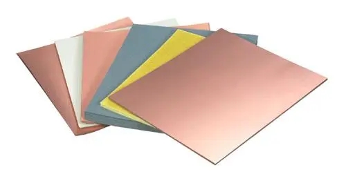
There are several types of materials used as substrates for PCBs. Some common materials include:

  1. FR-4: This is a substrate material widely used in PCBs. It is made of woven fiberglass cloth and epoxy resin, which has good electrical insulation and mechanical strength.
  2. Ceramics: Ceramic materials, such as alumina, can be used as substrates for PCBs. They have good thermal performance and are ideal for high power applications.
  3. Polyimide: This is a flexible heat-resistant material that is often used in flexible PCBs. It has good electrical and mechanical properties, but is not as strong as other materials.
  4. Metal core: Metal core PCB uses metal substrates, such as aluminum, copper or stainless steel as the base material. These PCBs have good thermal conductivity and are typically used in high power LED applications.
  5. Rogers: Rogers is a ceramic filled PTFE substrate with good high frequency electrical properties. It is commonly used in radio frequency applications such as antennas and high frequency circuits.
  6. Teflon: Teflon is a fluorine-containing polymer with low dielectric loss and good high-frequency performance. It is commonly used in microwave and millimeter wave applications.

These are just a few examples of materials used as PCB substrates. The choice of material depends on the specific requirements of the application, such as its intended use, frequency range, and thermal performance.

Factors affecting PCB quality

  1. Design quality: Design quality is crucial to determine the functionality and reliability of the PCB. Factors such as layout, routing, and component placement should be carefully considered.
  2. Manufacturing process: The quality of the manufacturing process can greatly affect the performance of the PCB. High-quality materials, sophisticated manufacturing processes, and strict quality control all ensure that PCBs are manufactured to a high standard.
  3. Component quality: The quality of components used on a PCB affects its reliability and lifespan. Using high-quality components ensures that the PCB will perform well for a longer period of time.
  4. Environmental factors: The use environment of PCB will also affect its quality. Factors such as temperature, humidity, and vibration can all affect the performance of a PCB.
  5. Testing and Validation: Proper testing and validation of the PCB ensures that it functions as intended and identifies and resolves any issues before the PCB is put into service.

Overall, ensuring the quality of a PCB requires attention to detail at each stage of the design, manufacturing, testing, and use process.

What are the types of PCBs?

There are many types of PCB (Printed Circuit Board) depending on the design and structure. Some common types include:

  1. Single-layer PCB: This PCB has only one layer of copper on a non-conductive substrate.
  2. Double layer PCB: This type of PCB has two copper layers separated by a non-conductive substrate.
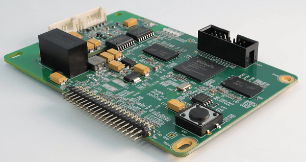
  3. Multilayer PCB: This PCB has multiple layers of copper and non-conductive substrates, which are laminated together.
  4. Rigid PCB: This type of board is made of rigid materials such as FR4 and cannot be bent.
  5. Flexible PCBs: These PCBs are made of flexible materials that can be bent or twisted along their length.
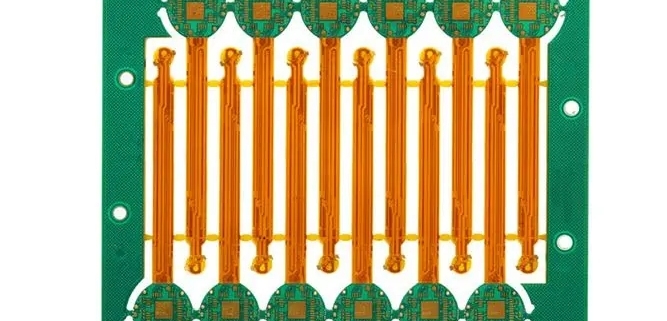
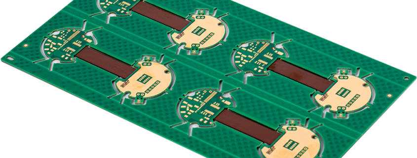
  6. Rigid-Flex PCB: This is a combination of Rigid and Flex PCB that allows components to be placed on both Rigid and Flex parts.
  7. High-frequency PCBs: These boards are designed to operate at very high frequencies, which makes them suitable for radio communications and other high-speed applications.
  8. Metal core PCB: This type of PCB has a metal core, which helps to dissipate heat and improve thermal management in high-power electronic applications.
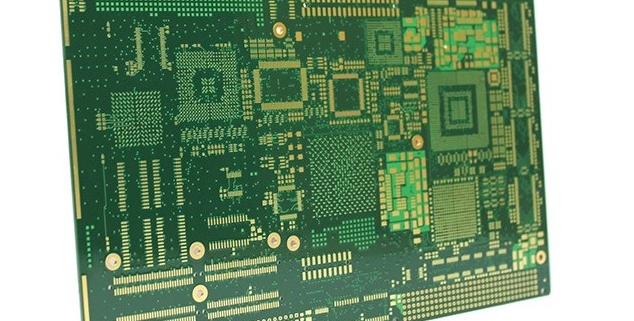
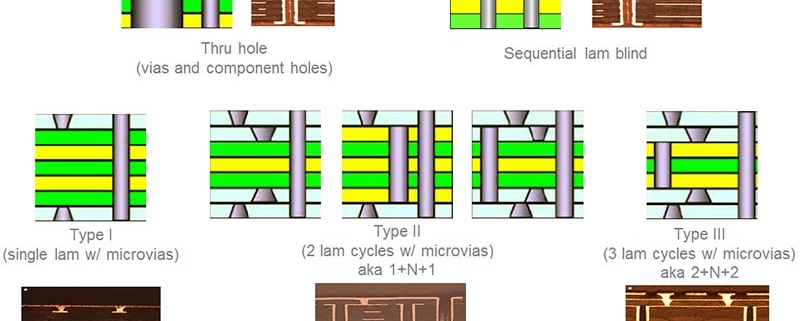
  9. HDI PCB: This stands for High Density Interconnect PCB, designed to have smaller and denser components, resulting in more compact and efficient electronics.

These are just a few examples of the various types of PCBs available. The type of PCB used for a particular application will depend on factors such as the complexity required, size and intended use of the electronic device.

Why choose high-precision HDI circuit board? Comprehensive analysis!

HDI, or High Density Interconnector, is an advanced printed circuit board (PCB) manufacturing technology. Its design and manufacturing process undergoes precise calculations and fine processing, and has many advantages, so it is very popular. Next, we will comprehensively analyze the reasons for choosing high-precision HDI circuit boards.
1. High-density wiring: HDI circuit boards have higher circuit density and smaller size, allowing denser wiring and more compact designs. This makes them particularly suitable for small devices or electronic products that require a high degree of integration, such as smartphones, tablets, etc.
2. Higher performance: HDI circuit boards can provide higher signal transmission speeds and lower signal delays because they can use shorter signal paths and smaller wiring spacing. This makes them ideal for high-speed digital signal transmission or high-frequency applications.
3. Enhanced signal integrity: HDI circuit boards can reduce signal crosstalk and signal attenuation, and improve signal integrity and stability. This is very important for complex circuit designs and applications requiring high performance.
4. Higher reliability: HDI circuit boards usually use more advanced manufacturing processes and materials, such as microvia technology, blind and buried via technology, etc., making them more reliable and stable. This can reduce product failure rates and extend product life.
5. Reduced costs: Although the manufacturing cost of HDI circuit boards may be slightly higher than traditional circuit boards, the overall product cost can be reduced due to its more compact design and higher performance. For example, HDI circuit boards can reduce the use of external connectors and components, thereby saving space and material costs.
6. Increased design freedom: HDI circuit boards enable more flexible and innovative designs because they enable more complex wiring and more compact component layouts. This allows designers to better realize their design concepts and meet clients’ specific needs.
Choosing high-precision HDI circuit boards can bring higher performance, better reliability and greater design freedom to product design, especially for applications that require high-density wiring, high-speed signal transmission and high-performance requirements. It is a very ideal choice.

How to solve the problem of component procurement?

There is a global shortage of components!
Our company has a strong component supply chain and have great advantages in purchasing components such as Infineon,NXP,ST, QUALCOMM, TEXASMICRON,Microchip  and so on.
Pls fell free to contact sales@bestpcb-ems.com if you need to purchase components,we guarantee original.
A promise is a promise!
If you are not in charge of purchasing components,pls do me a favor to forward this information to the keyperson.

We are very happy to solve the problem of component procurement for customers, and more than 5 new customers cooperate with us every month!

news cover 1

How to Cut PCB Assembly Cost Without Sacrificing Quality?

Many engineers, especially those just starting out, ask questions like “Where can I find the cheapest PCB assembly service?” or “How can I reduce my PCB assembly cost?” To tell the truth, there’s never any “cheapest” PCB assembly service. For those who only strive for low prices while neglecting PCB assembly quality, their projects may very likely fail due to low-quality circuit boards.

Although PCB assemblers are constantly trying to find ways to reduce circuit-board assembly cost to attract more business and ultimately gain more profit, price varies from one assembler to another. We strongly recommend you find a balance between assembly quality, customer service, and cost. The priority is to adjust your circuit design to reduce the assembly cost, and pinpoint the right PCB Assembler with the best overall service within your budget.

news cover 3

What are the Steps in the PCB Assembly Process?

Many of our valued customers contact us to learn the exact process . Our qualified engineers follow defined steps in the PCB assembly process. Our PCB assembly process include preparing the circuit board’s surface, placing the parts, soldering, cleaning and inspection & testing. Our trained assembly technicians diligently follow defined procedures and use modern methods of component placement for circuit board assembly.

We use both automated and manual techniques for placing PCB components. Generally, through-hole parts are placed manually whereas surface-mount components are placed with the use of a pick and place machine. Most of the time, automated assembly is not feasible for a small number of PCBs.

The soldering methods used by our team are wave-soldering for through-hole components and reflow soldering for surface-mount components. In the through-hole assembly process, the parts are placed on the PCB and wave-soldering is used to solder the leads for through-hole components. In the SMT assembly process, solder paste is applied via solder stencil on the PCB, then parts are placed on pads, and processed in a reflow oven to melt the solder paste. Furthermore, in mixed technology PCBs are both wave-soldered and reflowed.

After the circuit board is soldered, it is cleaned by our team. We use the latest techniques to clean the assembled circuit boards in order to remove all flux residue. Furthermore, different techniques are used to remove flux residue, which is generally a combination of cleaning agents, agitation, and heat. Then, the circuit board is sent for detailed inspection to check for accurate component placement.

State-of-the-art inspection tools are used to check the quality of the assembled boards. Some of the techniques used include sample checks, automated optical inspection (AOI), X-ray inspection, etc. After a thorough quality testing, the boards are delivered to the end customers.