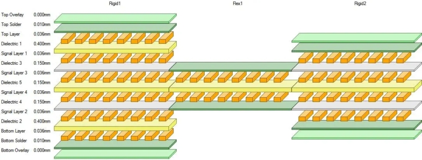
For most electronic components, common discrete component packages mainly include diodes, capacitors, resistors and transistors; common integrated circuits mainly include single in-line and dual in-line. At the same time, wires are connected to the pins of the package shell through the contacts on the chip, and these pins are connected to other devices through wires on the printed circuit board, thereby realizing the connection between the internal chip and the external circuit. Different components can use the same component package, and the same type of components can also have different packaging forms.
An important indicator to measure whether a chip packaging technology is advanced or not is: the ratio of chip area to packaging area. The closer this ratio is to 1, the better. The main factors to consider when packaging: the ratio of chip area to packaging area, in order to improve packaging efficiency, should be as close to 1:1 as possible. The pins should be as short as possible to reduce delay, and the distance between pins should be as far as possible to ensure that they do not interfere with each other and improve performance. Based on heat dissipation requirements, the thinner the package, the better. Packaging has roughly gone through the following development process: structural aspect: TO→DIP→PLCC→QFP→BGA→CSP. In terms of materials: metal, ceramics → ceramics, plastics → plastics. Lead shape: long lead straight insertion→short lead or leadless mounting→ball bump. Assembly method: through-hole insertion → surface assembly → direct installation.
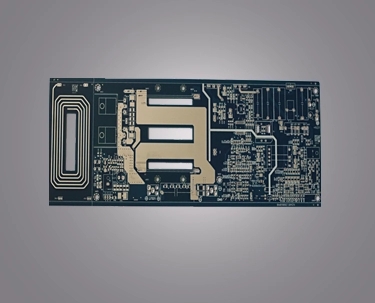
The following is an introduction to the specific packaging form:
SOP packaging technology was successfully developed by Philips Company from 1968 to 1969, and then gradually derived:
SOJ, J-lead small outline package
TSOP, Thin Small Outline Package
VSOP, Very Small Outline Package
SSOP, reduced SOP
TSSOP, thin reduced SOP
SOT, small outline transistor
SOIC, small outline integrated circuit
SOP/SOIC package
SOP is the abbreviation of English Small Outline Package, that is, small outline package.
DIP package
DIP is the abbreviation of “Double In-line Package” in English, that is, dual in-line package.
One of the plug-in packages, the pins are drawn from both sides of the package. The packaging materials are plastic and ceramic. DIP is the most popular plug-in package, and its application range includes standard logic IC, memory LSI, microcomputer circuits, etc.
PLCC package
PLCC is the abbreviation of “Plastic Leaded Chip Carrier” in English, which is plastic J-lead chip packaging.
The PLCC package has a square shape, a 32-pin package, and pins all around. The overall size is much smaller than the DIP package. PLCC packaging is suitable for installing wiring on PCB using SMT surface mounting technology. It has the advantages of small size and high reliability.
TQFP package
TQFP is the abbreviation of “Thin Quad Flat Package” in English, which is a thin plastic four-corner flat package. The four-sided flat packaging process can effectively utilize space, thereby reducing the space requirements for the printed circuit board.
Due to the reduced height and volume, this packaging process is ideal for applications with high space requirements, such as PCMCIA cards and network devices. Almost all ALTERA’s CPLD/FPGAs are available in TQFP packages.
PQFP package
PQFP is the abbreviation of “Plastic Quad Flat Package” in English, that is, plastic four-corner flat package.
The distance between the chip pins of the PQFP package is very small and the pins are very thin. Generally, large-scale or very large-scale integrated circuits adopt this packaging form, and the number of pins is generally more than 100.
TSOP package
TSOP is the abbreviation of “Thin Small Outline Package” in English, which is thin small size package. A typical feature of TSOP memory packaging technology is to make pins around the packaged chip. TSOP is suitable for installing wiring on PCB using SMT (surface mounting) technology.
The TSOP package shape has reduced parasitic parameters (output voltage disturbance caused when the current changes significantly), which is suitable for high-frequency applications. It is easier to operate and has higher reliability.
BGA package
BGA is the abbreviation of “Ball Grid Array Package” in English, which is ball grid array package. In the 1990s, with the advancement of technology, chip integration continued to increase, the number of I/O pins increased dramatically, power consumption also increased, and the requirements for integrated circuit packaging became more stringent. In order to meet the needs of development, BGA packaging began to be used in production.
Memory packaged with BGA technology can increase the memory capacity by two to three times while maintaining the same volume. Compared with TSOP, BGA has a smaller volume, better heat dissipation and electrical performance. BGA packaging technology has greatly improved the storage capacity per square inch. Memory products using BGA packaging technology are only one-third of the size of TSOP packaging with the same capacity. In addition, compared with the traditional TSOP packaging method, the BGA packaging method has a faster and more effective heat dissipation path.
The I/O terminals of the BGA package are distributed under the package in the form of circular or columnar solder joints in an array. The advantage of BGA technology is that although the number of I/O pins has increased, the pin spacing has not decreased but increased, thus Improved assembly yield. Although its power consumption increases, BGA can be welded using a controlled collapse chip method, which can improve its electrothermal performance. The thickness and weight are reduced compared with previous packaging technologies; the parasitic parameters are reduced, the signal transmission delay is small, and the frequency of use is greatly increased; coplanar welding can be used for assembly, and reliability is high.
QFP package
QFP is the abbreviation of “Quad Flat Package”, which is a small square flat package. QFP packaging was frequently used in early graphics cards, but there are few QFP packaged graphics memories with speeds above 4ns. Due to process and performance issues, they have been gradually replaced by TSOP-II and BGA. The QFP package has pins around the particle, which is quite obvious to identify. Four-side pin flat package. One of the surface mount packages, the pins are drawn out from four sides in a gull-wing (L) shape.
There are three types of base materials: ceramic, metal and plastic. In terms of quantity, plastic packaging accounts for the vast majority. When the material is not specifically indicated, in most cases it is plastic QFP. Plastic QFP is the most popular multi-pin LSI package. It is not only used in digital logic LSI circuits such as microprocessors and gate arrays, but also in analog LSI circuits such as VTR signal processing and audio signal processing.
The pin center distance is available in various specifications such as 1.0mm, 0.8mm, 0.65mm, 0.5mm, 0.4mm, 0.3mm, etc. The maximum number of pins in the 0.65mm center distance specification is 304.
TinyBGA package
When it comes to BGA packaging, we cannot fail to mention Kingmax’s patented TinyBGA technology. TinyBGA is called “Tiny Ball Grid” in English. It is a branch of BGA packaging technology and was successfully developed by Kingmax Company in August 1998. The ratio of the chip area to the packaging area is not less than 1:1.14, which can increase the memory capacity by 2 to 3 times without changing the memory size. Compared with TSOP package products, it has smaller size, better heat dissipation performance and electrical performance.
Memory products using TinyBGA packaging technology are only 1/3 of TSOP packaging with the same capacity. The pins of TSOP packaged memory are led from the periphery of the chip, while the pins of TinyBGA are led from the center of the chip. This method effectively shortens the signal transmission distance. The length of the signal transmission line is only 1/4 of the traditional TSOP technology, so the signal attenuation is also reduced. This not only greatly improves the anti-interference and anti-noise performance of the chip, but also improves the electrical performance. Chips using TinyBGA packaging can withstand FSBs up to 300MHz, while traditional TSOP packaging technology can only withstand FSBs up to 150MHz.
TinyBGA packaged memory is also thinner (package height is less than 0.8mm), and the effective heat dissipation path from the metal substrate to the heat sink is only 0.36mm. Therefore, TinyBGA memory has higher heat conduction efficiency, is very suitable for systems that run for a long time, and has excellent stability.