What should we pay attention to in high-frequency circuit board layout of PCB design?
With the rapid development of electronic technology and the widespread application of wireless communication technology in various fields, high-frequency, high-speed, and high-density have gradually become one of the important development trends of modern electronic products. The high-frequency and high-speed digitization of signal transmission forces PCBs to move towards micropores, buried/blind holes, fine conductors, and uniformly thin dielectric layers.
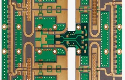
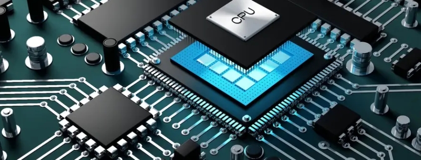
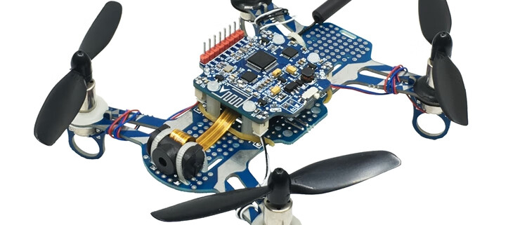
High frequency circuit board is a special type of circuit board with high electromagnetic frequency. Generally speaking, high frequency can be defined as a frequency above 1GHz. Its various physical properties, accuracy, and technical parameters require very high requirements, and are commonly used in fields such as automotive collision prevention systems, satellite systems, and radio systems. The high-frequency circuit board provided by the utility model is equipped with blocking edges that can block the flow of glue at the upper and lower opening edges of the hollow groove of the core board. In this way, when the core board is bonded with the copper clad board placed on its upper and lower surfaces, the flow of glue will not enter the hollow groove, and the bonding operation can be completed with one press. Compared with the high-frequency circuit board that requires two presses in existing technologies to complete, the high-frequency circuit board in the utility model has a simple structure, Low cost, easy to manufacture.
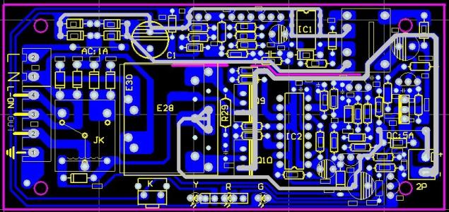
1. Reasonably select the number of layers
In PCB design, when wiring high-frequency circuit boards, the middle inner plane is used as the power and ground layers to provide shielding, effectively reduce parasitic inductance, shorten signal line length, and reduce cross interference between signals. Generally speaking, the noise of a four layer board is 20dB lower than that of a two layer board.
2. High frequency choke
When wiring high-frequency circuit boards in PCB design, high-frequency choke devices should be connected to common ground wires such as digital ground and analog ground. Generally, high-frequency ferrite magnetic beads with wires threaded through the center hole are used.
3. Signal line
When wiring high-frequency circuit boards in PCB design, signal routing cannot be looped and needs to be arranged in a daisy chain manner.
4. Inter layer wiring direction
In PCB design, when wiring high-frequency circuit boards, the interlayer wiring direction should be vertical, that is, the top layer should be horizontal and the bottom layer should be vertical, which can reduce interference between signals.
5. Number of through-holes
In PCB design, when wiring high-frequency circuit boards, the fewer vias, the better.
6. Copper coating
When wiring high-frequency circuit boards in PCB design, adding copper grounding can reduce interference between signals.
7. Decoupling capacitor
When wiring high-frequency circuit boards in PCB design, decoupling capacitors are connected across the power supply end of the integrated circuit.
8. Wiring length
When wiring high-frequency circuit boards in PCB design, the shorter the wiring length, the better, and the shorter the parallel distance between two wires, the better.
9. Land parcel
In PCB design, wrapping important signal lines can significantly improve the anti-interference ability of signals when wiring high-frequency circuit boards. Of course, it can also package the interference source so that it does not interfere with other signals.
10. Wiring method
In PCB design, when wiring high-frequency circuit boards, the wiring must be rotated at a 45 ° angle to reduce the transmission and mutual coupling of high-frequency signals.