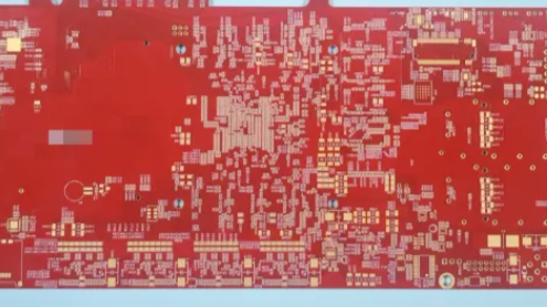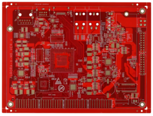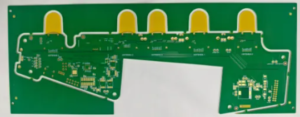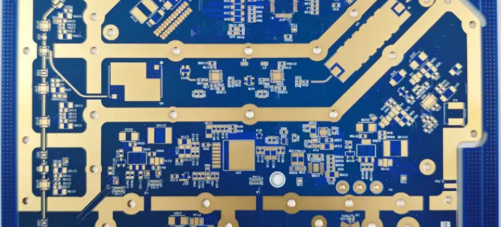
High speed! Panasonic Megtron 6 Material + resin plug hole + back drilling + gold finger, creating an extremely reliable “hard core” PCB!
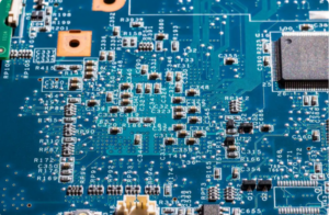
In cutting-edge fields such as 5G, high-speed servers, high-end industrial control, and precision medicine, the performance and reliability of PCBs directly determine the success or failure of end products.
Faced with the challenges of soaring signal rates, surging wiring density, and harsh working environments, ordinary boards and processes are no longer able to cope. How to break through?
The answer lies in the ultimate selection of materials and meticulous craftsmanship!

1. Cornerstone choice: Panasonic Megtron 6 – the “guardian” of signal integrity
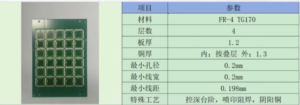
Top-level low loss: As a high-end member of Panasonic’s Megtron series, Meg6 has extremely low dielectric loss (Df) and stable dielectric constant (Dk). This means that when high-frequency and high-speed signals are transmitted, the signal attenuation is smaller and the distortion is lower, which effectively guarantees the purity and integrity of the signal. It is an ideal substrate for 10Gbps+ or even 25Gbps+ high-speed designs.
Excellent reliability: Megtron 6 board has excellent heat resistance (high Tg), low CTE (coefficient of thermal expansion) and long-term stability. In harsh environments such as high temperature, high humidity, cold and hot shock, it can still maintain stable electrical performance and mechanical strength, greatly reducing the risk of failure and extending product life.
Processing friendliness: Good drilling performance and chemical resistance provide a solid foundation for subsequent high-precision processing (such as back drilling and resin plugging).
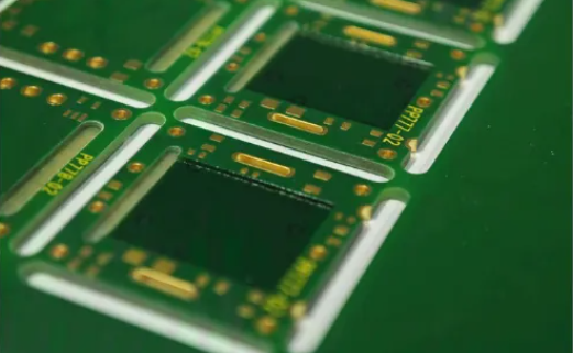
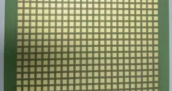
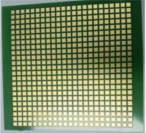
2. Precision filling: Resin plugging – “Minimally invasive experts” to eliminate hidden dangers
Solve pain points: Through holes on high-density boards (especially BGA areas), if there is residual air in the hole or the copper is not fully plated, it is very easy to cause “hole blowing” or “hole copper fracture” due to thermal expansion during reflow soldering, causing fatal defects.
Process essence: Resin plugging technology uses precision control to completely fill the inside of the through hole with specially formulated epoxy resin, and forms a solid support body after curing.
Core value: Eliminate hole blowing/board explosion, eliminate gas in the hole, provide structural support, and significantly improve thermal reliability.
Enhance planar connectivity: Provide a flatter and more solid pad surface for surface mounting (especially fine pitch BGA), reducing the risk of cold soldering.
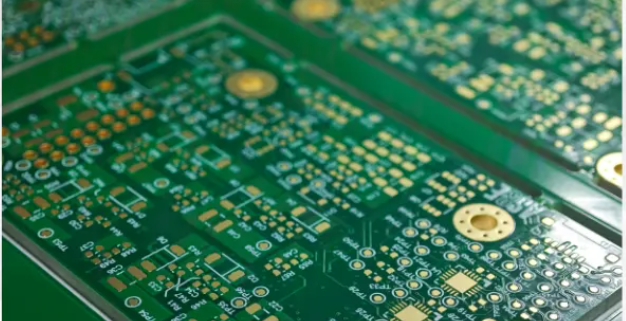
Conducive to high-density wiring: The surface after plugging is flat, and wiring can be safely carried out on it, freeing up valuable space and improving wiring freedom.

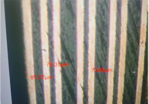
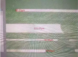
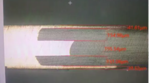
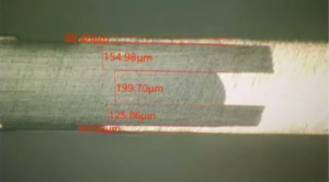
3. Signal purification: back drilling (controlled depth drilling) – the “scavenger” of high-speed signals
Signal killer – stubs: When the signal is transmitted from the surface layer to the inner layer through the via, the metal pillars (stubs) in the unconnected part of the hole are like an “antenna”, which will strongly reflect the high-speed signal and cause serious signal distortion (ringing, edge degradation), especially in the frequency band above GHz.
Precise removal: Back drilling technology uses a high-precision depth-controlled drill bit to accurately drill out the non-conductive and non-connecting stubs in the via.
Core value: Significantly improve signal quality: greatly reduce signal reflection and loss, improve signal rise time, and improve system bandwidth and stability.
Reduce crosstalk and EMI: eliminate unnecessary “antenna” effects, reduce noise radiation and interference.
High-speed design is one of the key processes to achieve signal integrity of ultra-high-speed digital circuits (such as server backplanes and high-speed SerDes channels).
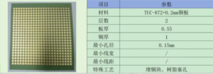
We are deeply involved in the field of high-end PCB manufacturing, and have mature experience in processing Panasonic Megtron 6 boards.
We can accurately control the filling fullness and surface flatness of the resin plug holes, equip with high-precision back drilling equipment to ensure accurate depth control, and strictly test the plating thickness, hardness and wear resistance of the gold finger. We are committed to providing a solid circuit board foundation for customers’ high-end, high-speed and high-reliability products.