BGA welding working principle, solder joint inspection and rework procedures.
Ball grid array (BGA) packaging has become one of the most popular technologies for integrated circuits requiring high input/output counts. BGA packaging has advantages over other methods due to its high-density interconnect capabilities. As integrated circuit complexity increases, and pin and gate counts continue to grow, BGAs become the optimal packaging solution to balance cost and performance. In this guide, we’ll explain BGA soldering – the process of attaching a BGA package to a printed circuit board. We’ll cover how BGA soldering works, solder joint inspection, and rework procedures. By understanding the ball grid array soldering process, its challenges and solutions, manufacturers can effectively leverage this advanced packaging technology.

What is BGA
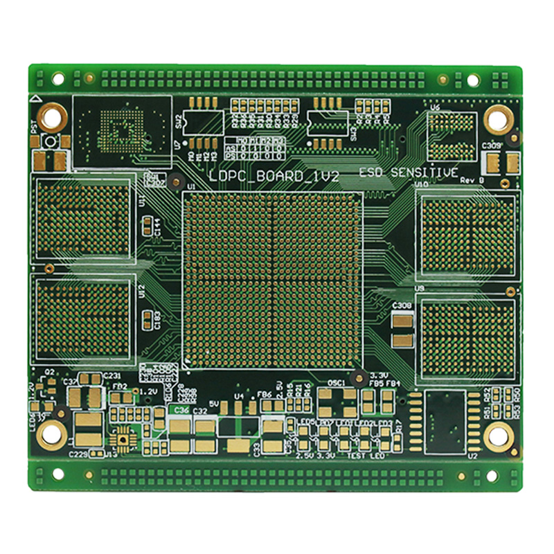
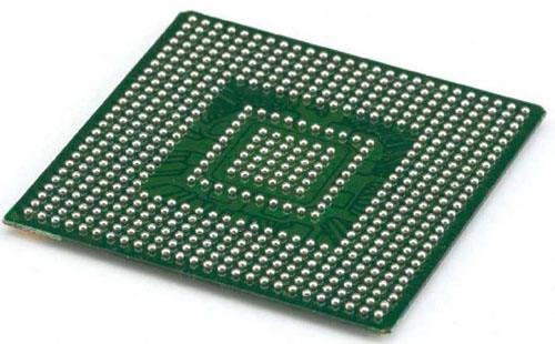
BGA is a unique surface mount package used to secure and mount SMD electronic components to integrated circuits on the surface of SMT printed circuit boards. BGAs have ball leads that are distributed in an array on the bottom of the package. And the ball array actually gets its name because it is an array of metal or alloy balls arranged in a grid.
BGA package is used to permanently mount the device. It provides more interconnect pins where you can place a flat or dual in-line package. The pins used in this technology are solder balls that are arranged in a pattern, usually a grid-like pattern, on the lower surface of the package. This is done to increase the connection area, not just the periphery. The most interesting thing is that with BGA soldering you have the benefit of using the entire underside of the device rather than just the perimeter.
This technology is used in various electronic products to install different integrated circuits such as FPGAs, WiFi chips, FPGAs, etc. What’s more, these packages are also used in RAM devices, PC chipsets, and microcontrollers.
How BGA soldering works
First, apply solder paste to the PCB pads that the BGA solder balls will contact. Solder paste is typically dispensed via a stencil or screen printing process to ensure accurate and repeatable application.
The BGA components are then precisely positioned and temporarily affixed to the PCB. This is accomplished using pick-and-place equipment with high-precision XY motion control and optical alignment systems. Proper alignment is critical.
PCB A is then fed into a reflow oven with a prescribed temperature profile. The solder paste melts, and the BGA’s solder balls melt and fuse with the PCB pads, forming solder joints. The profile must be hot enough to reflow the solder without damaging the components.
Finally, after cooling, check that the solder joints are formed correctly and have no defects. Any required rework is completed using specialized BGA rework equipment and procedures.
BGA solder joint inspection
When BGA packages were first introduced, there was uncertainty about how to verify solder joints because they were not visible underneath the component. Traditional optical inspection methods cannot be used. Additionally, electrical tests lack reliability because they only reflect the conductivity of the BGA at a specific moment of testing. This method cannot predict the long-term durability of the solder and may cause the solder joint to fail over time.
In order to truly inspect BGA solder joints, X-ray imaging technology is required. X-rays can penetrate components and capture images of hidden joints. Therefore, X-ray inspection is critical for process control and quality assurance when assembling circuit boards using BGAs. X-ray inspection provides the needed confidence by verifying that all joints are formed completely correctly. With X-rays, manufacturers can verify their BGA processes and ensure the long-term reliability required for these hidden interconnects.
BGA rework
When a BGA component is found to be defective, a rework process is required to remove and replace it. Solder joints must be carefully melted without disturbing adjacent components. This is achieved through a BGA rework station that utilizes targeted heat and airflow.
Infrared preheaters gently heat the circuit board from below to minimize thermal shock. Thermocouples monitor temperature in real time. After reflow, the vacuum tool lifts the BGA package. Strict process control is critical to success:
Match solder alloys to ensure joint compatibility
Balance bond strength for positioning adjustments
Strictly adhere to prescribed thermal curves
Use the minimum airflow setting required
Raise BGA slowly after reflow to avoid scrubbing
Choose a nozzle size that matches the component
With experience and rigorous procedures, reworked BGAs can become reliable. But it requires great precision and care to avoid collateral damage. Carefully tuned processes, specialized tools and operator skills are key drivers of high-quality BGA rework results.
final thoughts
Implementing a robust BGA soldering, inspection, and rework process requires investments in technical expertise, equipment, and operator training. But the advantages of higher-density BGA packaging make the effort worthwhile in terms of quality and performance. With expertise in precision printing, accurate placement, profile reflow, X-ray inspection and controlled rework, manufacturers like MOKO Technology enable customers to get the most out of BGAs in critical applications. As a leading PCB assembly supplier with nearly 20 years of experience, MOKO focuses on advanced ball grid array soldering technology. Please contact us today to discuss your specific BGA project and assembly requirements.

