4-layer step PCB, spray printed solder mask
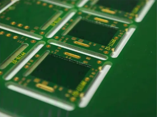
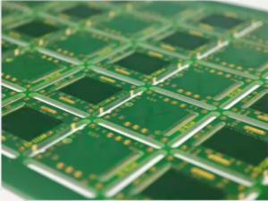
In the conventional step PCB products we make, the step position is generally treated with a window as the connection position of the components. As can be seen from the above picture, this product of ours has soldering done at the step position. The production of solder mask requires keeping the surface of the PCB work board flat, otherwise the silk screen ink will not cover it completely. Previously, the method we adopted was to silk screen the solder mask once before lamination. This method has great disadvantages. The ink after silk screen printing will become very brittle under lamination, and there is a high probability that the ink will fall off in the subsequent process. For this reason, we have thought of many solutions, but the effect is not very good.
After many attempts, our engineers came up with a solution, which is to use the principle of a character printer to print solder mask ink. No solder mask is applied before lamination, and solder mask is applied to the step part by printing after the finished product comes out. The result of the product is indeed satisfactory!
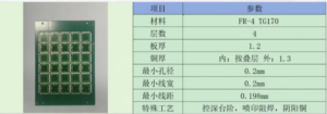
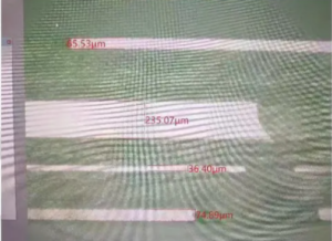
The above picture is the slice measurement data of our PCB. All aspects of the PCB data meet the customer’s requirements. In addition to the steps, this PCN also has yin and yang copper, half hole and other designs.


