3oz inner layer and 10oz outer layer/6oz inner layer and 6oz outer layer thick copper PCB
Thick copper PCB plays an important role in many fields with its high current carrying capacity, excellent thermal management performance and enhanced mechanical strength.
With the continuous development of electronic technology, the requirements for the current conduction and carrying capacity of circuit boards are getting higher and higher. Thick copper PCB has gradually become an important trend in the electronics field due to its unique material properties. Thick copper PCB mainly refers to the use of copper foil thicker than standard PCB in the manufacturing process. The copper thickness is usually 105 microns (3OZ) and above, and sometimes even up to 400 microns (12OZ).
Thick copper PCBs are widely used in the industrial field, especially in industrial automation, industrial robots, power supply systems, and renewable energy systems.
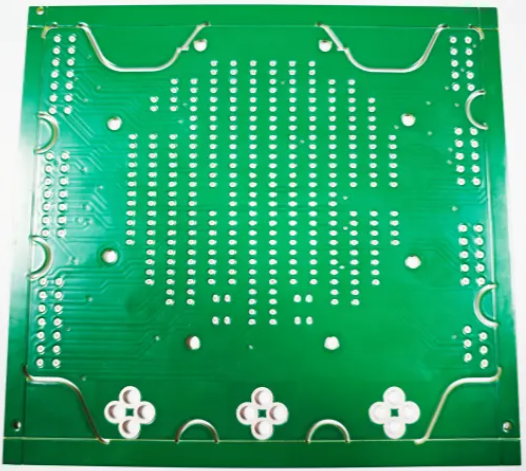
Today, SHENZHEN BEST PCBA CO., LIMITED introduces two thick copper PCBs. Both are 4-layer through-hole boards. The copper thickness requirements are 6OZ inside and 6OZ outside, and 3OZ inside and 10OZ outside! Let’s take a look at these two PCB:
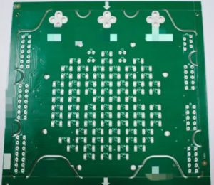
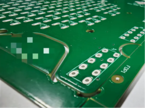
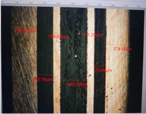
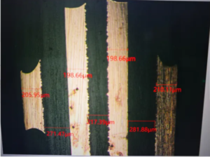
The dark green PCB is a product with 3OZ inside and 10OZ outside, and the light green PCB is a product with 6OZ inside and 6OZ outside. Let’s take a look at their slice diagrams:
The circuit design of thick copper PCB is relatively simple, but it is difficult to control the parameters during the production process!
Material selection: For 10OZ thick copper circuit boards, prepregs with high resin content need to be selected to ensure that the amount of glue flowing from the interlayer prepregs is sufficient to fill the inner layer graphics, while avoiding quality problems such as too thick insulating dielectric layers causing the finished board to be too thick or too thin, resulting in delamination, high-voltage test failure, etc.
Pressing production: The copper thickness of thick copper plates cannot be completed by electroplating and powering up like ordinary PCBs. The copper thickness of 10OZ is achieved by pressing 0.3mm copper plates on both sides of the core board, and then electroplating and powering up. The pressing of copper plates is much more difficult than that of copper foil.
Drilling production: When using special plates with high TG, high speed, high frequency, and thick copper, the difficulty of drilling roughness, drilling burrs, and drilling pollution is increased. The cumulative total copper thickness and board thickness of multilayer boards make it easy for drilling knives to break, and the problem of oblique drilling caused by board thickness is a production difficulty.
Circuit production: Due to the thick copper foil, it is difficult to etch out the complete circuit by conventional etching methods. Different factories have their own etching technology for thick copper PCBs. We also adjust the process for different products, accurately control the etching depth and shape, and ensure the quality of circuits and holes.

