14-layer thick copper PCB

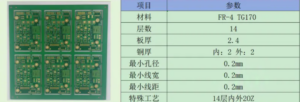
In the field of electronic circuits, the quality and performance of PCB directly affect the overall performance of electronic devices. We bring you a 14-layer thick copper board. Let us take a deeper look at the 14-layer PCB with both inner and outer layers of 2oz and appreciate its unique charm and advantages.

The 2oz copper foil thickness of the inner and outer layers gives this PCB excellent current carrying capacity. In high-power electronic devices, such as power supplies, motor drive devices, etc., it can easily cope with the transmission needs of large currents, effectively reduce line impedance, and reduce power loss, thereby improving the energy efficiency and stability of the equipment. Whether it is the core control board of industrial automation equipment or the power distribution board of high-end servers, 2oz copper thick PCB can provide reliable power support.

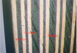
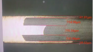
Let’s take a look at its slice diagram:

The 14-layer multi-layer structure design provides a good shielding and isolation environment for signal transmission. The reasonable layout and wiring between each layer, combined with the stability of 2oz copper foil, can effectively control signal transmission, crosstalk and other issues. For application scenarios with extremely high requirements for signal quality, such as high-speed digital circuits and radio frequency communication circuits, this PCB can ensure the integrity and accuracy of the signal, allowing high-speed and stable data transmission, laying a solid foundation for the high-performance operation of the equipment. For example, in the signal processing module of a 5G base station, it can ensure the fast and accurate interaction of massive data!

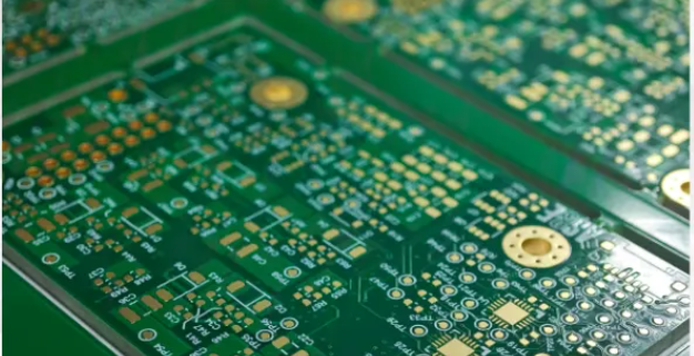
 

4-layer step PCB, spray printed solder mask

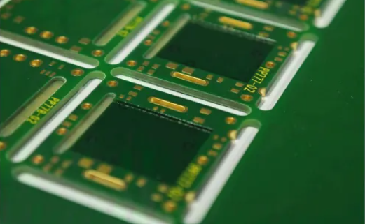
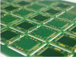
In the conventional step PCB products we make, the step position is generally treated with a window as the connection position of the components. As can be seen from the above picture, this product of ours has soldering done at the step position. The production of solder mask requires keeping the surface of the PCB work board flat, otherwise the silk screen ink will not cover it completely. Previously, the method we adopted was to silk screen the solder mask once before lamination. This method has great disadvantages. The ink after silk screen printing will become very brittle under lamination, and there is a high probability that the ink will fall off in the subsequent process. For this reason, we have thought of many solutions, but the effect is not very good.

After many attempts, our engineers came up with a solution, which is to use the principle of a character printer to print solder mask ink. No solder mask is applied before lamination, and solder mask is applied to the step part by printing after the finished product comes out. The result of the product is indeed satisfactory!

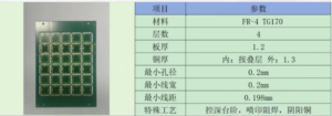
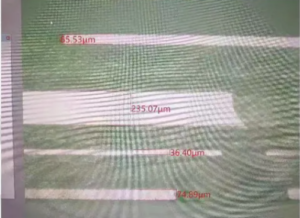
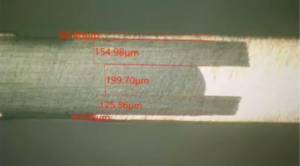
The above picture is the slice measurement data of our PCB. All aspects of the PCB data meet the customer’s requirements. In addition to the steps, this PCN also has yin and yang copper, half hole and other designs.

Buried copper block PCB is the cornerstone of circuit with excellent performance


The buried copper block PCB, literally speaking, means that copper blocks are buried inside the PCB. These copper blocks play a very important role in the circuit system. First of all, its excellent heat dissipation ability is a highlight. With the trend of increasingly miniaturized electronic devices and increasingly enhanced functions, the heating problem of electronic components is becoming more and more serious. The copper blocks in the buried copper block PCB have good thermal conductivity and can quickly conduct heat away to ensure that electronic components work at a suitable temperature. For example, in the PCB of a high-performance server, a large amount of data processing causes the chip to heat up seriously. The buried copper block design can effectively prevent the chip from overheating and causing performance degradation or damage.


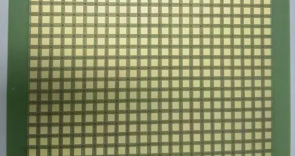
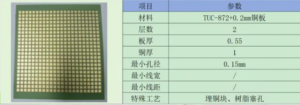
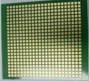
Today, we bring you a pure buried copper block PCB produced by BEST PCBA. The product does not have any complicated circuit production. The entire SET is made up of small copper blocks embedded on the board one by one. The base material of the product is a commonly used TUC-872 high-speed board. Different from conventional buried copper PCBs, the entire SET of our product is composed of copper blocks one by one. Direct etching will cause the copper blocks to scatter. During production, our engineers first etch the corresponding circuit pattern on the copper plate, and then press PP on the copper plate to fix the position of the copper block.


The above is a slice of our product. It is not difficult to see that the entire copper block is perfectly embedded in the board without any traces of splicing. The product has been perfectly delivered to the customer. If you encounter any problems in PCB production in the future, you can find BEST PCBA. Our strong team of engineers will do their best to serve you!