Special PCB board material product display

At present, most PCB substrates are made of FR-4 glass fiber substrate. This material has good insulation, corrosion resistance, high temperature resistance, and high cost performance, so most PCBs use this as the substrate.

However, for some products with specific electrical performance requirements, the performance of conventional substrates is not enough. These special properties require the use of some special substrates to meet them. Today, we will introduce some common special substrate products.

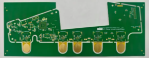
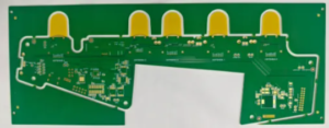
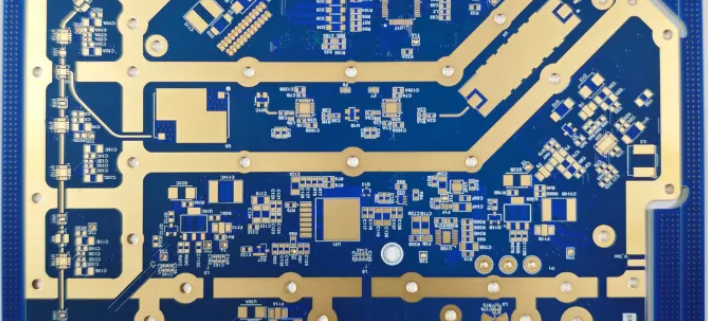
TUC  872LK


The above is an 8-layer HDI PCB of TUC872. TUC872 is a high-speed special board that we often use. It has a low dielectric constant, which is conducive to the transmission of high-speed signals. It also has a low dielectric loss factor, which means low energy loss during signal transmission, ensuring the strength of signal transmission!

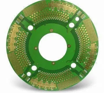
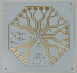
VT-901

This pancake-like PCB is made of VT-901 polyimide material. The ultra-high strength board performance enables the product to adapt to most harsh environments. Whether it is high temperature and high pressure, or low temperature and low pressure, it can perform its due functions well!

Rogers 4003C

RO4003 is a material with a hydrocarbon resin system and ceramic filler reinforced with woven glass cloth, and its electrical properties are close to those of PTFE/woven glass cloth materials. It is an excellent high-frequency PCB substrate with a stable dielectric constant. It can ensure the stability and accuracy of signal transmission in high-frequency circuits, and give the circuit good impedance control. It is widely used in microstrip line design, cellular base station antennas, point-to-point microwave communications, etc., and can ensure high-speed data transmission and stable signal coverage. For example, in the construction of 5G communication base stations, RO4003C can be used to make PCBs for base station antennas to meet the transmission requirements of 5G high-frequency signals.

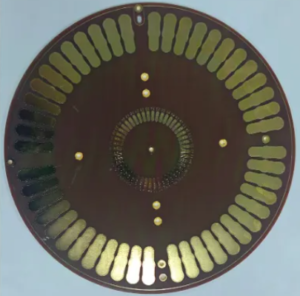
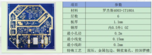
High frequency mixed pressing Copper paste plugging Deep groove control Metal edging PCB

With the rapid development of electronic technology today, PCB is the core component of electronic equipment, and its performance directly affects the quality and reliability of the entire electronic equipment. Most of the PCB products we usually see are made of a single core material, which is fine for conventional PCBs, but for some high-frequency and high-speed PCB products, the board value is relatively high. Mixing can save material costs. What we bring today is a Rogers 4003+IT180A mixed high-frequency PCB.

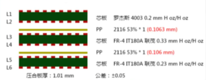
This product has a 6-layer PCB, L1-2 is high-frequency Rogers material, and L3-6 is conventional IT180 glass fiber material. This lamination structure saves material costs to a great extent while retaining the high-frequency performance of the product. However, mixed pressing is also a test of lamination technology. Core boards of different materials are prone to delamination during lamination, or layer deviation due to different expansion and contraction of the board. The lamination parameters of mixed pressing are more stringent than those of ordinary pressing.

The following figure is the pressing structure diagram of the product:

In addition, the product’s via process uses copper paste plugging. Copper paste has excellent electrical conductivity. In high-frequency and high-speed circuits, signal transmission has very strict requirements on conductivity. Copper paste plugging can effectively reduce the resistance and loss of signal transmission and ensure the integrity and accuracy of signal transmission.


PCB also has metal edging and controlled depth groove design. Metal edging can enhance the mechanical strength of the product, prevent edge wear, and have a certain electromagnetic shielding effect to prevent circuit signal interference. Controlled depth groove can facilitate the installation and fixation of components. Reasonable controlled depth groove design can reduce signal interference. By placing some sensitive components or signal lines in specific controlled depth grooves, electromagnetic interference with other components or signal lines can be avoided, improving the quality and stability of signal transmission.


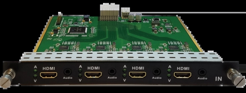
How to solve the delay problem of wireless HDMI adapter circuit board?

Latency issues with the wireless HDMI adapter circuit board may affect the synchronization of video and audio, especially in application scenarios that require real-time feedback. Here are some ways to solve latency issues:

1. Choose a low-latency wireless HDMI adapter: Some adapters on the market specifically advertise low latency features. Choosing such products can effectively reduce latency.

2. Update firmware and drivers: Make sure the adapter’s firmware and drivers are up to date. Manufacturers sometimes improve latency issues through firmware updates.

3. Adjust transmission parameters: Adjust parameters such as resolution, frame rate, and compression rate in the adapter’s settings to find the best latency balance.

4. Optimize wireless signals: Make sure the wireless signal is unobstructed, minimize obstacles, and use signal boosters or repeaters to extend the transmission range.

5. Use a wired connection: If the latency problem is very serious, consider using a wired HDMI connection as an alternative.

6. Use near-field communication (NFC): Some adapters support NFC, which can quickly pair devices and reduce latency during initial setup.

7. Restart devices: Restarting all related devices, including source devices, adapters, and display devices, can sometimes solve temporary latency issues.

8. Check power and connections: Make sure the power connections of all devices are stable, without power outages or voltage fluctuations.

9. Test different wireless channels: Wireless HDMI adapters usually support multiple wireless channels. Try using different channels to reduce interference.

10. Consult the manufacturer: If none of the above methods can solve the problem, you can contact the manufacturer’s customer service support for professional technical help.

Because the performance of the wireless HDMI adapter circuit board is affected by many factors, solving the delay problem may require trying multiple methods. In addition, as technology continues to develop, new solutions and products may continue to emerge.

How to solve the material compatibility problem in SMT patch processing?

The key to solving the material compatibility problem in SMT patch processing is to ensure that all materials used can remain stable during the processing and will not produce adverse reactions with each other. The specific analysis is as follows:

1. Choose the right solder paste. Solder paste matching: Select the right solder paste according to the heat capacity and welding temperature of the PCB board and components. Solder paste composition analysis: Ensure that the components in the solder paste are compatible with the metal plating of the PCB board and components to avoid adverse reactions.

2. Evaluate the heat resistance of the substrate material. Select a substrate material that can withstand the high temperature during the SMT patch processing to prevent the substrate from being deformed or damaged. Surface treatment suitability: Consider the substrate surface treatment process, such as tin spraying, OSP (organic protective agent), silver, etc., to ensure a good welding effect.

3. Consider the compatibility of component materials and component packaging materials: Check whether the packaging materials of the components can adapt to the automated production line of the SMT machine to avoid reduced production efficiency due to material incompatibility. Component heat resistance: Ensure that all components can withstand the high temperature during SMT patch processing to prevent component damage.

4. Optimize the process temperature curve optimization: adjust the temperature curve of reflow soldering according to the characteristics of different materials to ensure the quality of welding while avoiding material damage. Process control: implement strict process control, including the management of temperature and humidity in the production environment to reduce the instability of materials caused by environmental changes.

5. Conduct tests to verify compatibility tests: conduct small batch compatibility tests before formal production to verify the compatibility between different materials. Reliability testing: conduct comprehensive reliability tests on samples that have completed SMT patch processing, including but not limited to temperature cycle tests, mechanical impact tests, etc., to ensure long-term stability.

To solve the material compatibility problem in SMT patch processing, it is necessary to start from multiple angles and comprehensively consider the physical and chemical properties of various materials, which can effectively reduce the risks caused by material incompatibility and improve production efficiency and PCBA product quality.

What are the application cases of wireless charger circuit boards in different industries?

The application cases of wireless charger circuit boards in different industries are very extensive, covering multiple fields such as consumer electronics, automotive electronics, smart home, medical equipment and industrial applications. The following are some specific application cases:

Consumer electronics industry

1. Smartphones and tablets: Smartphones and tablets are one of the most common applications of wireless charger circuit boards. Users only need to place their mobile phones or tablets on the wireless charging pad to achieve a cable-free charging experience. This convenience makes wireless charging very popular in the consumer market.

2. Wearable devices: Wearable devices such as smart watches and wireless headphones also support wireless charging. These devices usually have a small battery capacity but a high frequency of use. The convenience of wireless charging is of great significance to improving user experience.

Automotive electronics industry

1. Wireless charging of electric vehicles: Wireless charging technology for electric vehicles is gradually maturing and commercializing. The wireless charging system is divided into a transmitter (installed on the ground or parking space) and a receiver (installed at the bottom of the electric vehicle). When the electric vehicle is parked in the charging area, the wireless transmission of electrical energy is achieved through the principle of electromagnetic induction. This technology reduces physical contact during charging and improves the convenience and safety of charging.

2. Car wireless charger: Many car PCB manufacturers have integrated wireless chargers in the car to facilitate drivers and passengers to wirelessly charge mobile phones and other devices. This design not only enhances the sense of technology in the car, but also avoids the problem of cable clutter caused by traditional wired charging.

Smart home industry

1. Wireless charging of smart home devices: In the field of smart home, wireless charging technology is also widely used in various smart devices. For example, smart speakers, smart door locks and other devices can be charged through wireless charging plates without frequent battery replacement or plugging and unplugging charging cables.

2. Furniture integrated wireless charging: Some high-end furniture such as coffee tables and bedside tables also integrate wireless charging functions. Users only need to place mobile phones and other devices on furniture to charge. This design not only improves the practicality of furniture, but also increases the convenience of home life.

Medical equipment industry

1. Wireless charging of medical instruments: In the field of medical equipment, wireless charging technology is used to charge various portable medical instruments. For example, electrocardiographs, blood glucose meters and other devices can be charged through wireless charging plates, avoiding the risk of cross infection that may be caused by traditional wired charging.

2. Wireless charging of medical robots: Medical robots such as surgical robots and nursing robots also use wireless charging technology. This technology allows robots to perform tasks without frequently returning to charging stations for charging, improving work efficiency and safety.

Industrial applications

1. Wireless charging of industrial equipment: In the industrial field, wireless charging technology is used to charge various industrial equipment. For example, robots, drones and other equipment on automated production lines can be charged through wireless charging pads, reducing manual intervention and downtime.

2. Wireless charging of industrial environment monitoring equipment: Some industrial environment monitoring equipment such as temperature sensors and humidity sensors also use wireless charging technology. These devices are usually deployed in inaccessible or dangerous environments. Wireless charging technology eliminates the need for maintenance personnel to frequently enter these environments for charging operations.

There are many application cases of wireless charger circuit boards in different industries. With the continuous advancement of technology and the reduction of costs, wireless charging technology will be widely used and promoted in more fields.