The development of PCB can be traced back to the 1950s, when it started with the quantitative production of some single-sided and double-sided PCBs. In the 1970s, multi-layer PCBs developed rapidly, and continued to move towards high precision, high density, and high reliability. This also laid the foundation for the rigid-flex board. In the birth and continuous development of FPC and PCB, a new product, the rigid-flex board, was born. It can be said that the rigid-flex board is the youngest member of the PCB family.
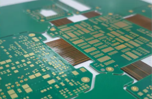
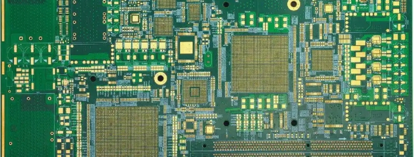
Early Rigid-Flex PCBs were mainly used in military and aerospace fields that have extremely high requirements for reliability and performance, such as aircraft, missiles and other high-end equipment. Today SHENZHEN BEST PCBA CO.,LIMITED bring you a 12-layer HDI Rigid-Flex PCB, let’s take a look at it first!
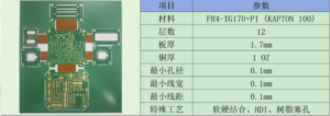
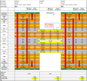
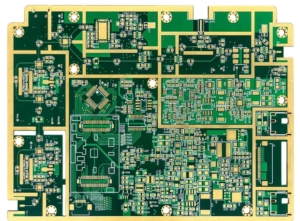
Rigid-flex boards can be said to be a beautiful work of art in PCB products! In the same level of rigid-flex boards, a variety of different stacking structures can be produced. For example, a 12-layer rigid-flex board can be a 10-layer rigid board + 2-layer flex board structure, or an 8-layer rigid board + 4-layer flex board structure, or a 6-layer rigid board + 6-layer flex board structure. The layer settings of soft and hard boards are not fixed, and can be set by engineers according to their needs! The internal structure of our 12-layer rigid-flex board is 8-layer rigid board + 4-layer flex board. Let’s appreciate its stacking structure:
L5-6, L7-8 are four-layer flex boards, and the other layers are FR4 rigid boards. In addition, this product is a 1 step blind and buried HDI. In order to ensure the stability and reliability of the product, we use plugged with resin technology to fill the buried hole part, and the blind hole part is filled with electroplating.
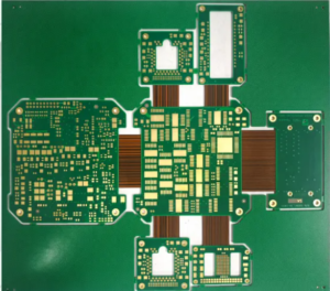
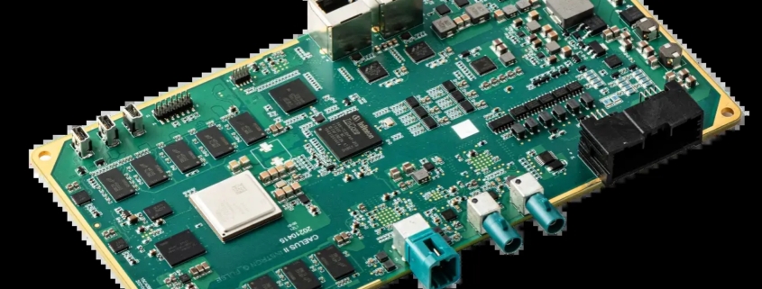
Of course, this product is not used in general electronic equipment. It is a PCB for industrial control equipment!
We delivered the product perfectly to our customers!
With the trend of miniaturization and complexity of modern electronic devices, the accuracy and rationality of the design of PCB printed circuit boards as a connecting bridge between electronic components are particularly important. The design of PCB is not only related to the stable performance of the product, but also directly affects the manufacturing cost and production efficiency. Among the many design rules, the minimum setting of PCB line spacing (the distance between line widths) and hole spacing (the distance from the edge of the hole to the adjacent wire) is one of the key factors to ensure the normal operation of the circuit, avoid short circuits and improve the success rate of manufacturing.
Overview of PCB line spacing and hole spacing PCB line spacing refers to the minimum allowable distance between the center lines of any two conductive lines on the PCB. This distance must be large enough to prevent accidental electrical connections (i.e. short circuits) caused by damage to insulating materials during the manufacturing process or when the circuit is running. The size of the line spacing is affected by many factors such as the materials used, manufacturing process, operating voltage, expected current, and expected working environment.
Hole spacing refers to the minimum allowable distance from the edge of the hole (via used to install component pins or realize interlayer connection) on the PCB to the edge of the nearest wire. Reasonable hole spacing design can ensure that the drilling and copper plating process will not damage the adjacent wires, while reducing the crosstalk between signals and ensuring the signal integrity of the circuit.
Why is the minimum spacing rule established?
1. Electrical safety: Too small line spacing and hole spacing may cause current leakage, causing short circuits, and in severe cases, damage the circuit board or even the entire system.
2. Manufacturing feasibility: Different manufacturing processes have their technical limitations, such as etching accuracy, drilling accuracy, etc. Too small spacing will increase the difficulty of manufacturing and reduce the yield rate.
3. Signal integrity: Electromagnetic interference is easily generated between conductors that are too close, affecting the quality of signal transmission, causing signal attenuation, delay or distortion.
4. Thermal management: Dense layout may hinder heat dissipation and affect the long-term reliability and life of components.
Factors affecting the minimum spacing Circuit operating voltage and current: High voltage or high current circuits require larger line spacing to reduce the risk of breakdown. Signal frequency: High-frequency signals are more sensitive to line spacing to reduce crosstalk and ensure signal quality. Manufacturing process: Advanced manufacturing technology can support smaller line spacing and hole spacing, but the cost increases accordingly. Environmental factors: such as temperature cycling, humidity, etc., require more conservative designs to improve reliability in harsh environments.
Design practice recommendations Follow manufacturer guidelines: Each PCB manufacturer will provide specific manufacturing capability parameters, including minimum line spacing and hole spacing requirements, which must be strictly followed during design. Use design software assistance: Modern PCB design software usually has a built-in DRC (design rule check) function to help designers automatically detect and adjust line spacing and hole spacing that do not meet specifications. Reserve margin: Under the premise of meeting performance requirements, appropriately increase line spacing and hole spacing to leave room for manufacturing tolerances and potential design modifications. Multilayer board design considerations: For multilayer boards, it is also necessary to consider the impact of inter-layer alignment and via penetration on adjacent layers for comprehensive design.
In short, the line spacing and hole spacing of PCBs are one of the most basic and critical design elements, which are directly related to the performance, reliability and manufacturing cost of the circuit board. By deeply understanding these rules and combining specific project requirements and manufacturing capabilities, designers can effectively avoid common design errors and create electronic products that are both efficient and reliable.
https://bestpcb-ems.com/wp-content/uploads/2024/09/srchttp___cbu01.alicdn.com_img_ibank_2017_045_448_4132844540_1942449778.jpgreferhttp___cbu01.alicdn.webp.jpg9371062administratorhttps://bestpcb-ems.com/wp-content/uploads/2023/05/logo-pcb2.pngadministrator2024-09-07 03:19:512024-09-07 03:20:05How to understand the minimum rules for PCB line spacing and hole spacing?
In order to optimize rail transit PCB to improve the stability and safety of train operation, the following aspects can be considered:
1. Improve the reliability and stability of PCB boards. Choose high-quality materials: Select PCB board materials with high reliability, long life and good heat resistance to ensure stable operation in harsh environments. Optimize manufacturing process: Through precise manufacturing process, reduce defects and defective rates in the manufacturing process and improve the overall quality of PCB boards. Redundant design: Redundant design is adopted in key components and signal transmission paths. Once a component fails, other components can take over the work to ensure continuous operation of the system.
2. Optimize the wiring design of PCB boards to reduce electromagnetic interference: Reasonably design the wiring to avoid cross interference and crosstalk between signal lines and reduce the impact of electromagnetic interference on system performance. Improve signal quality: Through reasonable wiring design, reduce signal attenuation and distortion, and improve the accuracy and reliability of signal transmission. Consider signal integrity: When transmitting high-speed signals, special attention should be paid to signal integrity issues, and appropriate topology and termination methods should be adopted to ensure signal quality.
3. Strengthen thermal management and arrange heat dissipation devices reasonably: Reasonably arrange heat dissipation devices such as heat sinks and heat pipes on PCB circuit boards to improve the conduction and dissipation efficiency of heat. Optimize the heat dissipation structure: Design a reasonable heat dissipation structure, such as increasing the heat dissipation area, using high-efficiency heat dissipation materials, etc., to ensure that the PCB board can work stably in a high temperature environment.
4.Enhance protection measures and select protective materials: Apply protective coatings or use protective materials on the surface of the PCB board to increase its ability to resist harsh environments, such as moisture-proof, dust-proof, and corrosion-proof. Conduct reliability tests: Conduct strict reliability tests during the design and manufacturing process to ensure that the PCB board can work normally under various harsh conditions.
5. Use intelligent technology to introduce intelligent monitoring: Integrate intelligent monitoring modules on the PCB board to monitor the operating status and parameters of the system in real time, and promptly discover and deal with potential problems. Intelligent scheduling and optimization: Combine big data and artificial intelligence technologies to intelligently schedule and optimize train operations to improve operating efficiency and safety.
6. Follow the fail-safe principle to design a fail-safe system: Follow the fail-safe principle in the design of the PCB board, that is, when a system or component fails, it can automatically switch to a safe state to prevent accidents. Strengthen fault detection and diagnosis: By improving fault detection and diagnosis capabilities, quickly and accurately locate the problem, and take appropriate measures to deal with it.
The above measures can significantly improve the performance and reliability of rail transit PCB boards, thereby ensuring the stability and safety of train operation.
https://bestpcb-ems.com/wp-content/uploads/2024/09/9.7.webp.jpg7841269administratorhttps://bestpcb-ems.com/wp-content/uploads/2023/05/logo-pcb2.pngadministrator2024-09-07 02:52:122024-09-07 03:00:49How to optimize rail transit PCB to improve train operation stability and safety?