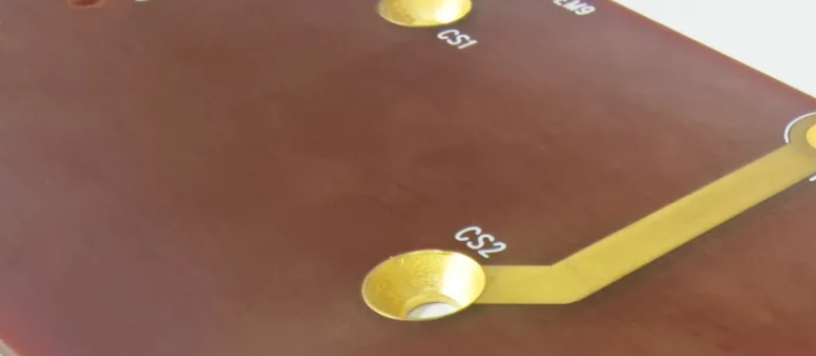
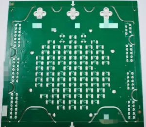
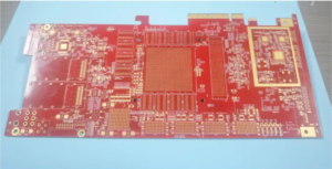
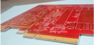
Optical Chip Carrier PCB

As science and technology develop, people’s observation of things is getting deeper and deeper. The product we bring today is an optical chip carrier used in single-photon SPAD imaging detectors. SPAD plays an important role in many fields, including but not limited to astronomy, particle size determination, quantum computing, quantum key distribution, single molecule detection, etc.

Regarding SPAD, interested friends can check the relevant information. Today, we mainly introduce this optical chip carrier PCB.

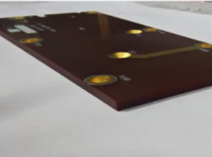
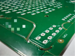
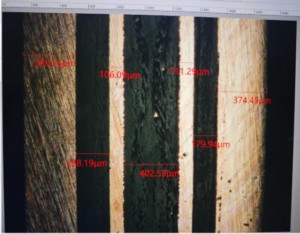
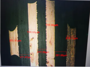
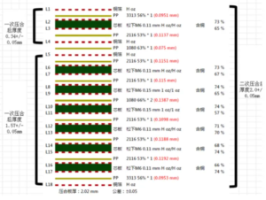
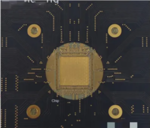
The most difficult part of the product process is these two steps, which require two depth control gongs and laser lid opening, and the depth control requirements are very strict.

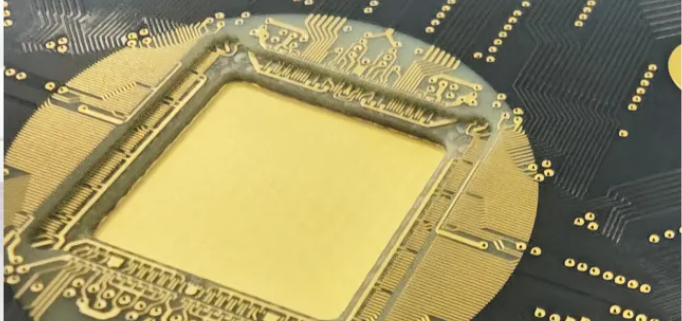
The surface treatment adopts the  ENEPIG process. The ENEPIG  has strong adhesion and is not easy to fall off, which improves the reliability and stability of the product.

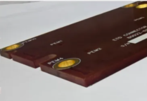
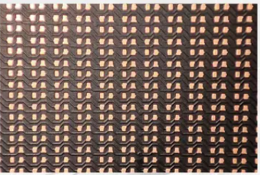
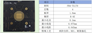
In addition, as a carrier board, the circuit design of the product is high-precision and highly integrated. The line width and line spacing are designed to be only 2mil. The minimum binding pad is 0.070mm.

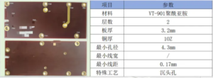
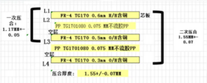
Although our product is only a 4-layer PCB, it needs to be pressed twice because of the steps. The following is the pressing structure diagram

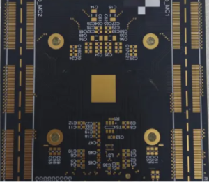
PCB carrier is a special printed circuit board used to carry electronic components, with the characteristics of high precision, high reliability and high integration. It has excellent electrical, mechanical and thermal properties, and can meet the high performance requirements of various complex electronic systems. Its process is not as complicated as imagined, but the parameter requirements at the detail level are very strict!

How to perform signal integrity analysis on FPC impedance board?

Conducting signal integrity analysis of FPC (Flexible Printed Circuit) impedance board is a complex process involving multiple steps and techniques. Here are some basic steps and considerations:

1. Understand the characteristics of FPC impedance board: First, you need to have a deep understanding of the material characteristics, design structure and working environment of FPC impedance board, all of which will affect the transmission and integrity of the signal.

2. Select appropriate test equipment: In order to accurately measure and analyze the signal, you need to select appropriate test equipment, such as oscilloscopes, spectrum analyzers, etc. These devices should have sufficient bandwidth and accuracy to capture and analyze high-speed signals.

3. Perform waveform testing: Waveform testing is the basis of signal integrity testing. Use an oscilloscope to measure the amplitude, rise time, fall time and other parameters of the signal to observe whether the signal is distorted or distorted. In addition, you can also analyze whether the edge time, jitter and other indicators of the signal meet the requirements.

4. Perform eye diagram testing: Eye diagram testing is a commonly used signal integrity test method that can help evaluate jitter, noise and other interference factors of the signal during transmission. Through the eye diagram test, you can determine whether the signal can remain stable and clear in a noisy and interfering environment.

5. Consider impedance matching: Impedance matching is critical for signal integrity. In the design of the impedance FPC board, the impedance matching of the transmitting and receiving ends should be ensured to reduce the reflection and distortion of the signal. In addition, attention should be paid to the continuity and consistency of the impedance to ensure that the signal remains stable throughout the transmission process.

6. Analyze the impact of capacitance on the signal: In the FPC impedance board, the capacitance will affect the transmission of the signal. For example, when a fast-rising step signal reaches the capacitor, the capacitor will charge quickly, which will affect the rise time and amplitude of the signal. Therefore, when analyzing signal integrity, the impact of capacitance on the signal needs to be considered.

7. Use simulation tools: Using simulation tools for signal integrity analysis is an effective method. These tools can simulate according to the design parameters and material properties of the FPC impedance board to predict the transmission performance and possible problems of the signal. Through simulation analysis, problems can be found and solved in the design stage, reducing the cost of later testing and modification.

8. Comprehensive evaluation: Finally, the signal integrity of the FPC impedance board needs to be comprehensively evaluated. According to the test results and the results of simulation analysis, it is judged whether the signal remains stable and clear during the transmission process and whether it meets the design requirements and application needs. If there are problems, corresponding optimization and improvement are required.

Signal integrity analysis of impedance board FPC requires comprehensive consideration of multiple factors, and the use of multiple test methods and simulation tools for analysis and evaluation. Only in this way can we ensure that the signal remains stable and clear during transmission and meet design requirements and application needs.


Explore the application of FPC multilayer boards in smart devices!

FPC multi-layer boards are increasingly used in smart devices. Its unique performance and design advantages have significantly improved the functionality, performance and user experience of smart devices. The following are some of the main uses of FPC multi-layer boards in smart devices. Application exploration:

Internal connection and wiring: In smart devices such as smartphones and tablets, FPC multilayer boards are widely used for the connection and wiring of internal components. The multilayer design allows for more complex circuit layouts within a limited space, thereby improving the integration and reliability of the device. At the same time, the flexible nature of FPC allows greater flexibility in the design and manufacturing process of the device, helping to achieve a thinner, lighter, and more compact product design.

Touch screen and display module: FPC multilayer boards play an important role in touch screen and display modules. They can connect display screens, touch screen controllers and other key components to achieve high-quality image transmission and touch response. Due to the thinness and flexibility of FPC soft boards, they can easily adapt to various screen sizes and shapes, providing excellent visual and interactive experience for smart devices.

Sensors and camera modules: In smart devices, various sensors and camera modules require stable and reliable circuit connections. FPC multilayer boards can provide such connections and ensure high-speed data transmission and accuracy. In addition, the flexible characteristics of FPC can also help sensors and camera modules adapt to different installation positions and angles, thereby improving the applicability and flexibility of the equipment.

Power management and battery systems: FPC multilayer boards are also widely used in power management and battery systems. They can connect key components such as batteries, chargers, and power management chips to achieve efficient energy transmission and management. By optimizing the power management system, FPC multilayer boards can improve the battery life and charging efficiency of the device, bringing a better user experience.

Modular design: The modular design of FPC multilayer boards makes smart devices more convenient to upgrade, repair and expand. By connecting different functional modules through FPC multilayer boards, the equipment can be expanded and upgraded more flexibly. In addition, since FPC is very easy to install and repair, users can easily replace or upgrade a module in the device, thereby extending the service life of the device and reducing maintenance costs.

The application of FPC multilayer boards in smart devices provides devices with higher integration, reliability, flexibility and user experience. With the continuous development and popularization of smart devices, the application prospects of FPC multilayer boards will become more and more broad.


What are the considerations in FPV camera circuit board design?

There are many aspects to consider when designing FPV camera circuit boards, which are related to the performance, stability and final application scenarios of the circuit board. Here are some key design considerations:

1. Processor performance: The circuit board should use a high-performance processor that can quickly process images and flight data to meet the real-time and response speed requirements of FPV cameras.

2. Sensor integration: Integrate high-quality sensors such as gyroscopes and accelerometers to ensure the stability and accuracy of the aircraft during high-speed flight. For photography purposes, special sensors such as magnetometers and barometers for stable video may also need to be integrated.

3. Power management: Design an efficient power management system to support fast and frequent speed changes. At the same time, considering the need for long-term shooting, ensure continuous and stable power output.

4. Signal transmission: Optimize signal transmission design to support long-distance and low-latency signal transmission to ensure that pilots can respond to track conditions or obtain clear images in real time.

5. Interface configuration: Configure sufficient PWM outputs and UART ports according to application requirements to connect various actuators, servo mechanisms, cameras and other imaging devices.

6. Firmware function: Develop firmware with multiple flight modes and tuning options to suit different tracks and flying styles or specialized image processing and video recording functions.

7. Heat dissipation design: Since long-term high-speed operation may cause overheating, a good heat dissipation system needs to be designed to prevent overheating.

8. Durability design: Considering the possibility of impact and collision, the design of the circuit board should be more robust, especially the circuit board for racing. The circuit board for photography may pay more attention to protective measures such as waterproof and dustproof.

The design of the FPV camera circuit board needs to comprehensively consider multiple aspects such as processor performance, sensor integration, power management, signal transmission, interface configuration, firmware function, heat dissipation design and durability to ensure that the circuit board is used in the FPV camera to achieve the best performance and stability.


What is the development history of rail transit PCB boards?

The development history of rail transit PCB boards is a story closely linked to the advancement of electronic technology. From early electronic connections to modern complex control systems, PCB boards play an increasingly important role in rail transit. The following is a detailed introduction to its development history:

1. Pioneer of technological innovation in the early development stage: The history of PCB boards can be traced back to the early 20th century, when they were mainly used to simplify circuit connections in electronic devices. With the development of semiconductor technology, PCB boards began to be used in a wider range of fields, including early communication equipment and computer systems. The foundation of the electronics manufacturing industry: The emergence of PCB boards has greatly improved the reliability and production efficiency of electronic equipment, becoming the basic components of the electronics manufacturing industry. Their design and application are constantly optimized to adapt to the ever-changing needs of electronic technology.

2. Mid-term application expansion promoted by communication technology: With the development of communication technology, PCB boards have been used in signal transmission and control systems of rail transit. These systems require high reliability and stability, and the design of PCB boards has become more sophisticated and complex. Assistance of automatic control: The automatic control of rail transit systems requires complex circuit design and fast signal processing, in which PCB boards play a key role. They not only ensure the accuracy of the signal, but also improve the response speed and efficiency of the system.

3. The trend of modern technology integration with high-density integration: In order to adapt to the needs of modern rail transit systems for miniaturization and high performance, the design of PCB boards tends to be high-density integrated, which means that more electronic components can be integrated into a smaller space, thereby improving the overall performance and reliability of the system. The importance of thermal management: Since rail transit vehicles generate a lot of heat during operation, the thermal management of PCB boards has become increasingly important. Reasonable thermal design can effectively prevent components from overheating and ensure the stable operation of the system.

4. Future development direction Innovation in materials science: In order to further improve the performance of PCB boards, future development trends include the use of new materials and technologies, such as nanomaterials and advanced manufacturing processes. These innovations are expected to improve the conductivity, heat resistance and mechanical strength of PCB boards. Intelligent integration: With the development of artificial intelligence and Internet of Things technologies, future PCB boards will be more intelligent and able to achieve self-diagnosis and remote monitoring, which will provide rail transit systems with a higher level of safety and maintenance convenience.

The development of rail transit PCB boards reflects the progress and innovation of electronic technology. From the early simple circuits to the current highly integrated and intelligent systems, PCB boards have been improving the safety and efficiency of rail transit. With the continuous advancement of technology, PCB circuit boards will continue to play a key role in the field of rail transit, bringing a safer, more convenient and efficient travel experience.

How to effectively deal with common quality problems of HDI circuit boards?

In the rapidly developing field of electronic manufacturing, high-density interconnect (HDI) circuit boards have become the core components of many electronic products due to their excellent performance and wide application. However, HDI circuit boards often encounter some quality problems during the manufacturing process. How to effectively deal with these problems is the key to improving product quality and ensuring market competitiveness.

Common quality problems and causes

Circuit breakage and short circuit: Due to the high integration and precision design of HDI boards, the circuit spacing is small, and the slightest carelessness during processing may cause circuit breakage or short circuit.

Poor welding: Problems such as loose welding points, cold welding, etc. will seriously affect the electrical performance and reliability of HDI boards.

Material problems: The quality of materials such as substrate materials, copper foil, and solder mask ink is unstable, which will lead to the overall performance of HDI boards.

Improper process control: Improper control of key processes such as etching, drilling, and electroplating will also lead to quality problems.

Effective response strategy

Optimized design and reasonable process design: Fully consider the characteristics of HDI boards in the design stage, reasonably layout the circuits, and avoid overly compact designs.

Process optimization: According to the characteristics of HDI boards, optimize key processes such as etching, drilling, and electroplating to ensure processing accuracy and stability.

Strict material screening and control Supplier selection: Select reputable and quality-guaranteed suppliers to ensure the quality of raw materials. Material testing:

Strictly test the raw materials entering the factory to ensure that they meet the standards. Strengthen process control and quality testing Process monitoring: Establish a complete process control system to monitor and record key processes in real time. Quality testing: Introduce advanced testing equipment to conduct comprehensive and detailed quality testing of HDI boards.

Improve employee skills and awareness Skill training: Strengthen employee skills training to improve employees’ understanding and response capabilities to HDI board quality issues. Quality awareness: Improve employees’ quality awareness so that every employee understands the importance of quality.

Establish a quality management system System establishment: Establish a complete quality management system, from design, raw materials, production to testing, each link has clear standards and processes. Continuous improvement: Through regular quality reviews and internal audits, problems are discovered and continuously improved.


The response to HDI circuit board quality issues requires us to start from multiple aspects, including optimizing design and process, strict material screening and control, strengthening process control and quality testing, improving employee skills and awareness, and establishing a quality management system. Only in this way can we ensure that the quality of HDI circuit boards is stable and reliable and meets market demand.

VT-901 Aerospace Multilayer PCB

In the PCB industry, FR-4 glass fiber is selected as the most common board material in the industry due to its good high temperature resistance and corrosion resistance. However, in addition to FR-4, there are some other materials that are also indispensable in PCB manufacturing due to their unique characteristics. We collectively refer to these materials as special materials. Special materials play an important role in the electronics industry, especially in the fields of communication equipment, automotive electronics, medical equipment, industrial control and automation. These special materials not only improve the performance of PCBs, but also enhance the reliability of electronic products.


Today,SHENZHEN BEST PCBA CO.,LIMITED  bring you a PCB product made of VT-901 polyimide as the base material! At present, the special boards commonly used on the market are some high-frequency and high-speed types, such as Panasonic, Rogers, and Taiyao. Everyone is familiar with them, and these boards are relatively easy to purchase on the market. VT-901 polyimide, some friends may not know what kind of board this is. Now let me introduce it to you.

On January 30, 2024, Tenghui Electronics (Suzhou) Co., Ltd. announced that its VT-901 polyimide (PI) material has been exclusively certified by the European Space Agency (ESA) and can be used for the Belgian ACB Group to manufacture high-density interconnect printed circuit boards (HDI). This also makes ACB the only printed circuit board (PCB) manufacturer that can provide HDI technology in the ESA qualified field.

VT-901PI material meets ESA standards and is suitable for the stringent requirements of ACB’s HDI board manufacturing process. It has a high heat resistance temperature of 395°C, a high TG of 250°C, and a low axial CTE of 50. It meets the IPC4101E Appendix A inspection standards for aerospace materials. The same professional equipment is also used to manufacture laminates (designed for the most demanding aerospace circuit boards).


I believe everyone knows that any PCB designed for the aerospace field has very strict performance requirements! As a trustworthy PCB manufacturer, it is definitely an honor if your products can be used in the aerospace field!


3oz inner layer and 10oz outer layer/6oz inner layer and 6oz outer layer thick copper PCB

Thick copper PCB plays an important role in many fields with its high current carrying capacity, excellent thermal management performance and enhanced mechanical strength.
With the continuous development of electronic technology, the requirements for the current conduction and carrying capacity of circuit boards are getting higher and higher. Thick copper PCB has gradually become an important trend in the electronics field due to its unique material properties. Thick copper PCB mainly refers to the use of copper foil thicker than standard PCB in the manufacturing process. The copper thickness is usually 105 microns (3OZ) and above, and sometimes even up to 400 microns (12OZ).

Thick copper PCBs are widely used in the industrial field, especially in industrial automation, industrial robots, power supply systems, and renewable energy systems.
Today, SHENZHEN BEST PCBA CO., LIMITED introduces two thick copper PCBs. Both are 4-layer through-hole boards. The copper thickness requirements are 6OZ inside and 6OZ outside, and 3OZ inside and 10OZ outside! Let’s take a look at these two PCB:


The dark green PCB is a product with 3OZ inside and 10OZ outside, and the light green PCB is a product with 6OZ inside and 6OZ outside. Let’s take a look at their slice diagrams:


The circuit design of thick copper PCB is relatively simple, but it is difficult to control the parameters during the production process!

Material selection: For 10OZ thick copper circuit boards, prepregs with high resin content need to be selected to ensure that the amount of glue flowing from the interlayer prepregs is sufficient to fill the inner layer graphics, while avoiding quality problems such as too thick insulating dielectric layers causing the finished board to be too thick or too thin, resulting in delamination, high-voltage test failure, etc.

Pressing production: The copper thickness of thick copper plates cannot be completed by electroplating and powering up like ordinary PCBs. The copper thickness of 10OZ is achieved by pressing 0.3mm copper plates on both sides of the core board, and then electroplating and powering up. The pressing of copper plates is much more difficult than that of copper foil.

Drilling production: When using special plates with high TG, high speed, high frequency, and thick copper, the difficulty of drilling roughness, drilling burrs, and drilling pollution is increased. The cumulative total copper thickness and board thickness of multilayer boards make it easy for drilling knives to break, and the problem of oblique drilling caused by board thickness is a production difficulty.

Circuit production: Due to the thick copper foil, it is difficult to etch out the complete circuit by conventional etching methods. Different factories have their own etching technology for thick copper PCBs. We also adjust the process for different products, accurately control the etching depth and shape, and ensure the quality of circuits and holes.


HDI Light Board

In today’s digital age, LED displays have become an indispensable element in the fields of information display, advertising, and event hosting. One of the key technologies that supports this visual feast is high-quality PCB boards. PCB is the “skeleton” of electronic products, while the PCB of LED displays is its “soul”.

In indoor and outdoor display screens, 2-layer or 4-layer applications are the most common. Small pitch LED display screens use more layers of circuit boards to meet the requirements of high-density signal transmission. In transparent LED display screens, technology research and development continues to advance to reduce costs and improve efficiency.

The wiring density of the inner and outer layers of the PCB for LED display screens is extremely high. Generally, the minimum line width and line spacing of the inner and outer layers is 3.5mil. The design characteristics of COB-type LED display screens determine that the minimum line width and line spacing are required to be 2.5mil, and the corresponding outer copper thickness is recommended to be 1OZ to ensure the yield of dense lines. This requires precise control of the line width and spacing during the production process to ensure the normal function and high-quality display of the display screen.

SHENZHEN BEST PCBA CO., LIMITED has invested a lot of time and energy in the research and development and production of LED screen light board PCB, continuously optimizing the production process and improving the process capability of the light board!

For some conventional transparent screens and large-pitch lamp bead PCBs, our yield rate can now reach over 90%. For small-pitch through-hole lamp boards, we can guarantee that all orders with a pitch of P1.95 or above will be delivered in one go. For HDI lamp boards, the minimum lamp bead pitch we can produce is P0.98!

Our company currently has very good leadership in all kinds of straight screens, special-shaped screens, first-order and second-order HDI light boards, with an overall yield rate of over 75%!

18-layer mechanical blind hole + step + back drilling + immersion gold + gold plating 30U + M6 high-speed circuit board

With the development of science and technology, information and communication technology are changing with each passing day, and people’s requirements for computer performance are getting higher and higher. Correspondingly, the hardware requirements for computer communication equipment are also getting higher and higher. PCB is the basic product of electronic equipment, and its high-end precision determines the performance of the entire finished computer communication equipment!

Today, SHENZHEN BEST PCBA CO., LIMITED brings you an FPGA acceleration card for high-performance computing and network acceleration devices. Let’s first take a look at what the PCB board looks like.

The bright red solder mask ink, immersion gold + electroplated gold finger 30U” surface treatment process make the whole product look very high-end. But what really attracts people to this product is not just its appearance, but its complex design and precise production process.
First of all, let’s take a look at its step process.


The conventional step process is to use non-flowing glue PP to press and stack the layers in the step part. And our product needs to achieve a high-speed effect, so the whole board uses Panasonic M6 PCB high-speed board, but there is no non-flowing glue PP corresponding to M6 on the market. We can only use flowing glue PP for pressing, which is very challenging for the production of step parts.
In addition, this product is also an 18-layer mechanical blind hole board. Let’s take a look at the pressing structure diagram

The motherboard of the product is divided into two boards, L1-4 and L5-18, and the finished product is made after three laminations. The lamination of multi-layer boards is extremely difficult, and the lamination of multi-layer special board products must be controlled in detail. The result of a mistake is that all the previous efforts are wasted!
Finally, in order to ensure the transmission of high-speed signals, reduce signal attenuation, ensure that the signal is stronger and more reliable, and also to prevent signal distortion problems, we also added back drilling technology in product production.
CKT-1 drills from the top layer to the bottom layer with a depth of 1.25+/-0.05, CKB-1 drills from the bottom layer to the top layer with a depth of 0.35mm and a depth of 1.45+/-0.05, 0.351mm with a depth of 1.25+/-0.05, 0.352mm with a depth of 1.05+/-0.05, and 0.353mm with a depth of 0.2+/-0.05.