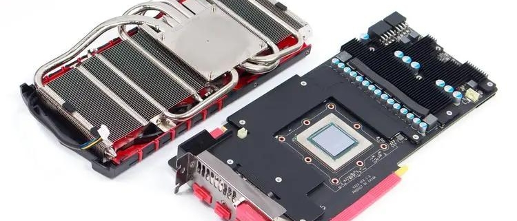
As 5G construction continues to advance, industrial fields such as precision microelectronics and aviation and shipbuilding have further developed, and these fields all cover the application of PCB circuit boards. With the continuous development of these microelectronics industries, we will find that the manufacturing of electronic components is gradually becoming miniaturized and thinner, and the requirements for precision are getting higher and higher. As the most commonly used processing technology in the microelectronics industry, laser welding is bound to There are increasingly higher requirements for the welding level of PCB circuit boards.
Inspection after PCB circuit board welding is very important for both enterprises and customers. In particular, many enterprises have strict requirements for electronic products. If inspection is not done, performance failures will easily occur, affecting product sales, corporate image and word of mouth. The laser welding equipment produced by Shenzhen Zichen Laser has fast efficiency, high welding yield, and post-weld inspection function, which can meet the welding processing and post-weld inspection needs of enterprises. So, how to check the quality of PCB circuit board after welding? Below Zichen Laser shares several commonly used detection methods.
01 PCB triangulation
What is triangulation? That is, the method used to check the three-dimensional shape. At present, the triangulation detection method has been developed and used and equipment capable of detecting its cross-sectional shape has been designed. However, because this triangulation detection method is incident from different lights and in different directions, the observation results will be different. Essentially, objects are inspected through the principle of light diffusion. This method is the most appropriate and most effective. As for the situation where the welding surface is close to mirror surface conditions, this method is inappropriate and difficult to meet production needs.
02 Light reflection distribution measurement method
This method mainly uses the welding part to detect the decoration, injects light inward from an oblique direction, sets a TV camera above, and then inspects it. The most important part of this operation method is how to know the surface angle of the PCB solder, especially how to know the irradiation photometric information. The angle information must be captured through various light colors. On the contrary, if it is illuminated from above, the angle measured is the reflected light distribution, and just check the tilted surface of the solder.
03 Change the angle for camera inspection
How to detect PCB after welding? To use this method to detect the quality of PCB after welding, a device with a changing angle is necessary. This device generally has at least 5 cameras, multiple LED lighting equipment, uses multiple images, and uses visual inspection conditions for inspection, so the reliability is relatively high.
04 Focus detection utilization method
For some high-density circuit boards, after PCB welding, the above three methods are difficult to detect the final result, so the fourth method, which is the focus detection and utilization method, needs to be used. This method is divided into multiple methods, such as the multi-stage focus method, which can directly detect the height of the solder surface and achieve high-precision detection. If 10 focus surface detectors are set up at the same time, the focus surface can be obtained by seeking the maximum output and detect The position of the solder surface. If it is detected by irradiating the object with a fine laser beam, a lead device with a pitch of 0.3mm can be successfully detected by staggering 10 specific pinholes in the Z direction.
https://bestpcb-ems.com/wp-content/uploads/2024/07/673.jpg325460administratorhttps://bestpcb-ems.com/wp-content/uploads/2023/05/logo-pcb2.pngadministrator2024-07-04 03:30:142024-07-04 03:30:18How to check the quality of PCB circuit board after laser welding?
Ball grid array (BGA) packaging has become one of the most popular technologies for integrated circuits requiring high input/output counts. BGA packaging has advantages over other methods due to its high-density interconnect capabilities. As integrated circuit complexity increases, and pin and gate counts continue to grow, BGAs become the optimal packaging solution to balance cost and performance. In this guide, we’ll explain BGA soldering – the process of attaching a BGA package to a printed circuit board. We’ll cover how BGA soldering works, solder joint inspection, and rework procedures. By understanding the ball grid array soldering process, its challenges and solutions, manufacturers can effectively leverage this advanced packaging technology.
What is BGA
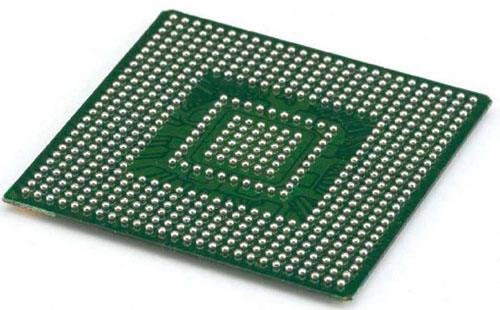
BGA is a unique surface mount package used to secure and mount SMD electronic components to integrated circuits on the surface of SMT printed circuit boards. BGAs have ball leads that are distributed in an array on the bottom of the package. And the ball array actually gets its name because it is an array of metal or alloy balls arranged in a grid.
BGA package is used to permanently mount the device. It provides more interconnect pins where you can place a flat or dual in-line package. The pins used in this technology are solder balls that are arranged in a pattern, usually a grid-like pattern, on the lower surface of the package. This is done to increase the connection area, not just the periphery. The most interesting thing is that with BGA soldering you have the benefit of using the entire underside of the device rather than just the perimeter.
This technology is used in various electronic products to install different integrated circuits such as FPGAs, WiFi chips, FPGAs, etc. What’s more, these packages are also used in RAM devices, PC chipsets, and microcontrollers.
How BGA soldering works
First, apply solder paste to the PCB pads that the BGA solder balls will contact. Solder paste is typically dispensed via a stencil or screen printing process to ensure accurate and repeatable application.
The BGA components are then precisely positioned and temporarily affixed to the PCB. This is accomplished using pick-and-place equipment with high-precision XY motion control and optical alignment systems. Proper alignment is critical.
PCB A is then fed into a reflow oven with a prescribed temperature profile. The solder paste melts, and the BGA’s solder balls melt and fuse with the PCB pads, forming solder joints. The profile must be hot enough to reflow the solder without damaging the components.
Finally, after cooling, check that the solder joints are formed correctly and have no defects. Any required rework is completed using specialized BGA rework equipment and procedures.
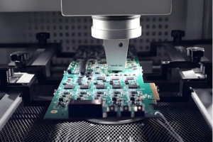
BGA solder joint inspection
When BGA packages were first introduced, there was uncertainty about how to verify solder joints because they were not visible underneath the component. Traditional optical inspection methods cannot be used. Additionally, electrical tests lack reliability because they only reflect the conductivity of the BGA at a specific moment of testing. This method cannot predict the long-term durability of the solder and may cause the solder joint to fail over time.
In order to truly inspect BGA solder joints, X-ray imaging technology is required. X-rays can penetrate components and capture images of hidden joints. Therefore, X-ray inspection is critical for process control and quality assurance when assembling circuit boards using BGAs. X-ray inspection provides the needed confidence by verifying that all joints are formed completely correctly. With X-rays, manufacturers can verify their BGA processes and ensure the long-term reliability required for these hidden interconnects.
BGA rework
When a BGA component is found to be defective, a rework process is required to remove and replace it. Solder joints must be carefully melted without disturbing adjacent components. This is achieved through a BGA rework station that utilizes targeted heat and airflow.
Infrared preheaters gently heat the circuit board from below to minimize thermal shock. Thermocouples monitor temperature in real time. After reflow, the vacuum tool lifts the BGA package. Strict process control is critical to success:
Match solder alloys to ensure joint compatibility
Balance bond strength for positioning adjustments
Strictly adhere to prescribed thermal curves
Use the minimum airflow setting required
Raise BGA slowly after reflow to avoid scrubbing
Choose a nozzle size that matches the component
With experience and rigorous procedures, reworked BGAs can become reliable. But it requires great precision and care to avoid collateral damage. Carefully tuned processes, specialized tools and operator skills are key drivers of high-quality BGA rework results.
final thoughts
Implementing a robust BGA soldering, inspection, and rework process requires investments in technical expertise, equipment, and operator training. But the advantages of higher-density BGA packaging make the effort worthwhile in terms of quality and performance. With expertise in precision printing, accurate placement, profile reflow, X-ray inspection and controlled rework, manufacturers like MOKO Technology enable customers to get the most out of BGAs in critical applications. As a leading PCB assembly supplier with nearly 20 years of experience, MOKO focuses on advanced ball grid array soldering technology. Please contact us today to discuss your specific BGA project and assembly requirements.
https://bestpcb-ems.com/wp-content/uploads/2024/07/671.jpg800800administratorhttps://bestpcb-ems.com/wp-content/uploads/2023/05/logo-pcb2.pngadministrator2024-07-04 03:16:432024-07-04 03:16:48BGA welding working principle, solder joint inspection and rework procedures.
In the electronics manufacturing industry, PCB (Printed Circuit Board) board serves as a “neural network” connecting electronic components, and its quality directly affects the performance and stability of the entire electronic device. As a common manufacturing problem, half-hole copper deficiency in PCB boards has complex causes and far-reaching consequences. This article will deeply analyze the reasons for the lack of copper in the half-hole of the PCB board and discuss its possible impact.
1. Analysis of the causes of lack of copper in half holes of PCB boards
Drilling process issues
Insufficient precision of drilling equipment: Low-precision drilling equipment may result in inconsistent hole sizes, rough or damaged hole walls.
Drill bit selection and wear: Unsuitable drill bits or excessively worn drill bits will affect the quality of drilling.
Improper drilling parameter settings: Unreasonable settings such as feed speed, rotation speed, etc. will also cause damage to the hole wall.
Electroplating copper process issues
Electroplating solution composition and concentration: The copper ion concentration in the electroplating solution is too low or too high, which may affect the electroplating effect.
Electroplating solution temperature and pH value: Improper temperature or pH value will affect the adhesion and uniformity of the electroplated copper layer.
Current density and time: The current density is too high or too small, and the plating time is too short or too long, which will lead to poor copper layer quality.
plate problem
Uneven material of the board: There are impurities or inconsistent fiber directions inside the board, which will affect the adhesion and uniformity of the electroplated copper layer.
Improper plate pretreatment: If the pretreatment process such as oil removal and rust removal is not in place, it will affect the subsequent electroplating effect.
Operational and Management Issues
Insufficient operator skills: The skill level of operators directly affects product quality.
Strict quality inspection: Strict quality inspection of semi-finished products and finished products may cause problematic products to flow into the next process.
2. The impact of lack of copper in the half hole of PCB board
Reduced electrical performance: Lack of copper in half holes can lead to poor circuit connections, increase resistance, and reduce the electrical performance of electronic devices.
Reduced equipment stability: Poor circuit connections may cause short circuits, open circuits and other faults during operation of the equipment, reducing the stability and reliability of the equipment.
Increased production costs: The lack of copper in half holes will increase the scrap rate and repair rate of products, leading to an increase in production costs. At the same time, more time and resources may need to be invested in technical improvements and quality control to solve this problem.
Damage to market competitiveness: PCB board quality issues are an important factor affecting a company’s brand image and reputation. If the product has quality problems such as half-hole copper shortage, it will affect customers’ trust in the company and reduce market competitiveness.
3. Solution Strategies and Suggestions
Improve equipment and process level: introduce advanced drilling equipment and electroplating equipment, optimize process parameter settings, and ensure the stability and reliability of the drilling and electroplating process.
Strictly screen and inspect boards: Strictly screen and inspect the base materials of PCB boards to ensure that the quality of the boards meets the requirements. At the same time, the pretreatment process control of the plate is strengthened to ensure that the hole wall is clean and free of impurities.
Strengthen operation and management training: improve the skill level of operators and strengthen the rigor of quality inspection. Establish a complete quality traceability system to promptly trace and analyze problematic products.
Adopt new technologies and new materials: Explore the use of new technologies and new materials to improve the manufacturing quality and performance of PCB boards. For example, advanced technologies such as laser drilling technology and nano-plating technology are used to improve product accuracy and reliability.
The lack of copper in the half hole of the PCB board is a problem that needs attention. By in-depth analysis of its causes and adopting effective solution strategies, we can reduce the incidence of half-hole copper shortage problems, improve the quality and performance of PCB boards, and thereby enhance the market competitiveness of enterprises.
https://bestpcb-ems.com/wp-content/uploads/2024/07/670.jpg10001361administratorhttps://bestpcb-ems.com/wp-content/uploads/2023/05/logo-pcb2.pngadministrator2024-07-04 03:05:142024-07-04 03:05:19Analysis of the causes of lack of copper in half holes of PCB boards and their effects!
In electronics manufacturing, the stability and reliability of PCBs (Printed Circuit Boards) are crucial. The PCB ink hole plugging process is one of the key steps to ensure circuit board performance. It involves using special ink to fill conductive holes to prevent short circuits between different layers. This article will delve into the PCB ink plugging process and share how to ensure the stability and reliability of the circuit board through this process.
1. The importance of PCB ink plug holes
Prevent short circuit: Different conductive layers can be effectively isolated through plug holes to avoid short circuit caused by current leakage.
Ensure signal integrity: Good hole plugging technology can reduce interference during signal transmission and maintain signal clarity and stability.
Improved mechanical strength: The circuit board after plugging the holes can better withstand physical stress and improve the overall mechanical stability.
2. Key measures to ensure stability and reliability
Choose the right ink: Depending on the application needs of the circuit board, choose an ink with good electrical insulation, high adhesion, and good chemical resistance.
Precisely control the plugging process: Strictly control the temperature, pressure and time during the plugging process to ensure that the ink is fully filled and solidified.
Use high-quality equipment: Use high-precision plugging equipment to improve the quality and efficiency of plugging.
Implement strict quality inspection: comprehensively inspect the plugging effect through methods such as automatic optical inspection (AOI) and X-ray inspection.
3. Strategies for optimizing hole plugging process
Optimize design layout: Consider the need for hole plugging during the design stage to avoid an overly dense hole layout and ensure that the ink can be fully filled.
Conduct material compatibility testing: Conduct compatibility testing on inks and sheets before production to ensure that their interaction meets requirements.
Regularly maintain equipment: Regularly maintain and calibrate plughole equipment to maintain optimal performance.
Continuous process improvement: Based on production feedback and reliability test results, the hole plugging process is continuously optimized to improve the quality of the circuit board.
PCB ink plugging process is a key link to ensure the stability and reliability of the circuit board. By choosing the right inks, precisely controlling the hole plugging process, using high-quality equipment, and implementing strict quality inspections, manufacturers can effectively improve the performance of their circuit boards. At the same time, optimizing design layout, conducting material compatibility testing, regular maintenance of equipment and continuous improvement of processes will further ensure the long-term stability and reliability of circuit boards. With the continuous advancement of electronic technology, the requirements for PCB manufacturing are becoming higher and higher, which requires manufacturers to continuously innovate and improve plug hole technology to meet the challenges of the future electronics industry.
https://bestpcb-ems.com/wp-content/uploads/2024/07/666-1.jpeg7951080administratorhttps://bestpcb-ems.com/wp-content/uploads/2023/05/logo-pcb2.pngadministrator2024-07-04 02:54:132024-07-04 02:54:17Discussion on PCB ink plugging process: How to ensure the stability and reliability of the circuit board!
With the rapid development of science and technology, electronic products have become increasingly popular. As the core component of electronic products, the importance of PCB boards (printed circuit boards) is self-evident. Among the many PCB board types, 4-layer PCB boards have attracted much attention due to their excellent performance and wide range of application fields.
Price factors of customized 4-layer PCB board
The price of customized 4-layer PCB boards is affected by many factors, including the following aspects:
Plate selection: The prices of plates of different materials and thicknesses vary greatly. Generally speaking, high-performance boards are more expensive but offer better electrical performance and mechanical strength.
Design complexity: The higher the design complexity, the more difficult the processing and the cost will increase accordingly. For example, PCB boards that require more process steps such as drilling and milling will be more expensive.
Production batch: The larger the production batch, the lower the single-chip cost. Because in mass production, equipment and human resources can be fully utilized to reduce unit costs.
Delivery time: If the customer has strict requirements on delivery time, additional expedited fees may be required.
Cost and performance trade-offs for 4-layer PCB boards
When choosing a custom 4-layer PCB board, we need to make a trade-off between cost and performance. Here are some factors worth considering:
Performance requirements: We need to clarify the performance requirements of the product. If the product has higher requirements on electrical performance, stability, reliability, etc., then we should choose higher performance boards and more sophisticated design solutions, but this may increase the cost.
Budget constraints: After clarifying the performance requirements, we need to consider budget constraints. If the budget is limited, we need to reduce costs as much as possible while meeting performance requirements. This may require us to make compromises in plate selection, design complexity, etc.
Delivery Time: Delivery time is also a factor to consider. If customers have strict requirements on delivery time, we may need to choose faster production processes and more expensive plates to ensure on-time delivery. But it can also increase costs.
The price of customized 4-layer PCB boards is affected by many factors, including board selection, design complexity, production batch size, and delivery time. When choosing a custom 4-layer PCB board, we need to make a trade-off between cost and performance to meet the product’s performance needs and budget constraints. By referring to the price list and considering various factors, we can choose the customized 4-layer PCB board that best suits our needs.
https://bestpcb-ems.com/wp-content/uploads/2024/07/589.png32003351administratorhttps://bestpcb-ems.com/wp-content/uploads/2023/05/logo-pcb2.pngadministrator2024-07-04 02:52:322024-07-04 02:52:37Cost and performance trade-off of 4-layer PCB board!
For electronic equipment, a certain amount of heat will be generated during operation, causing the internal temperature of the equipment to rise rapidly. If the heat is not dissipated in time, the equipment will continue to heat up, and the device will fail due to overheating. The reliability of electronic equipment Performance will decrease.
Therefore, it is very important to handle the heat dissipation of the circuit board well. The heat dissipation of PCB circuit board is a very important link. So what are the heat dissipation techniques of PCB circuit board? Let’s discuss it together.
01
Heat dissipation through the PCB board itself. The currently widely used PCB boards are copper-clad/epoxy glass cloth base materials or phenolic resin glass cloth base materials, and there are also a small amount of paper-based copper-clad sheets.
Although these substrates have excellent electrical properties and processing properties, they have poor heat dissipation. As a heat dissipation path for high-heating components, it is almost impossible to expect the PCB resin itself to conduct heat, but to dissipate heat from the surface of the component to the surrounding air.
However, as electronic products have entered the era of component miniaturization, high-density installation, and high-heat assembly, it is not enough to rely solely on the surface of components with very small surface areas to dissipate heat.
At the same time, due to the extensive use of surface-mounted components such as QFP and BGA, the heat generated by the components is transferred to the PCB board in large quantities. Therefore, the best way to solve the problem of heat dissipation is to improve the heat dissipation capacity of the PCB itself that is in direct contact with the heating components, through the PCB board Conduct or radiate out.
▼Add heat dissipation copper foil and use large-area power supply ground copper foil
▼Thermal vias
▼The copper is exposed on the back of the IC to reduce the thermal resistance between the copper and the air
PCB layout
Heat-sensitive devices are placed in the cold air area.
The temperature detection device is placed in the hottest location.
Devices on the same printed board should be arranged according to their heat generation and heat dissipation degree as much as possible. Devices with small heat generation or poor heat resistance (such as small signal transistors, small-scale integrated circuits, electrolytic capacitors, etc.) should be placed in the cooling air flow. At the top of the cooling air flow (at the entrance), devices with high heat generation or good heat resistance (such as power transistors, large-scale integrated circuits, etc.) are placed at the bottom of the cooling air flow.
In the horizontal direction, high-power devices should be placed as close to the edge of the printed board as possible to shorten the heat transfer path; in the vertical direction, high-power devices should be placed as close to the top of the printed board as possible to reduce the impact of these devices on the temperature of other devices when they are working. .
The heat dissipation of printed boards in equipment mainly relies on air flow, so the air flow path must be studied during design and the devices or printed circuit boards should be reasonably configured.
When air flows, it always tends to flow in places with low resistance, so when configuring devices on a printed circuit board, avoid leaving a large air space in a certain area. The same issue should also be paid attention to in the configuration of multiple printed circuit boards in the whole machine.
Devices that are more sensitive to temperature are best placed in the area with the lowest temperature (such as the bottom of the device). Never place it directly above the heating device. It is best to arrange multiple devices staggered on the horizontal plane.
Place the devices that consume the most power and generate the most heat near the best locations for heat dissipation. Do not place high-heat components in the corners and edges of the printed board unless a heat sink is arranged nearby.
When designing the power resistor, choose a larger device as much as possible, and make sure there is enough space for heat dissipation when adjusting the printed board layout.
Component spacing recommendations:
02
Add radiators and heat conduction plates to high-heating devices. When there are a few devices in the PCB that generate a large amount of heat (less than 3), you can add radiators or heat pipes to the heating devices. When the temperature cannot be lowered, you can use Radiator with fan to enhance cooling effect.
When there are a large number of heating devices (more than 3), a large heat dissipation cover (board) can be used. It is a special radiator customized according to the position and height of the heating device on the PCB board or placed on a large flat-panel radiator. Cut out the high and low positions of different components. Attach the heat dissipation cover to the component surface and make contact with each component to dissipate heat.
However, due to the poor consistency of the components during assembly and soldering, the heat dissipation effect is not good. Usually, a soft thermal phase change thermal pad is added to the component surface to improve the heat dissipation effect.
03
For equipment that uses free convection air cooling, it is best to arrange the integrated circuits (or other devices) vertically or horizontally.
04
Use reasonable wiring design to achieve heat dissipation. Since the resin in the board has poor thermal conductivity, and copper foil lines and holes are good conductors of heat, increasing the remaining rate of copper foil and adding thermal holes are the main means of heat dissipation. To evaluate the heat dissipation capability of PCB, it is necessary to calculate the equivalent thermal conductivity (nine eq) of the insulating substrate for PCB, which is a composite material composed of various materials with different thermal conductivity.
05
Devices on the same printed board should be arranged according to their heat generation and heat dissipation degree as much as possible. Devices with small heat generation or poor heat resistance (such as small signal transistors, small-scale integrated circuits, electrolytic capacitors, etc.) should be placed in the cooling air flow. At the top of the cooling air flow (at the entrance), devices with high heat generation or good heat resistance (such as power transistors, large-scale integrated circuits, etc.) are placed at the bottom of the cooling air flow.
06
In the horizontal direction, high-power devices should be placed as close to the edge of the printed board as possible to shorten the heat transfer path; in the vertical direction, high-power devices should be placed as close to the top of the printed board as possible to reduce the impact of these devices on the temperature of other devices when they are working. .
07
The heat dissipation of printed boards in equipment mainly relies on air flow, so the air flow path must be studied during design and the devices or printed circuit boards should be reasonably configured.
When air flows, it always tends to flow in places with low resistance, so when configuring devices on a printed circuit board, avoid leaving a large air space in a certain area.
The same issue should also be paid attention to in the configuration of multiple printed circuit boards in the whole machine.
08
Devices that are more sensitive to temperature are best placed in the area with the lowest temperature (such as the bottom of the device). Never place it directly above the heating device. It is best to arrange multiple devices staggered on the horizontal plane.
09
Place the devices that consume the most power and generate the most heat near the best locations for heat dissipation. Do not place high-heat components in the corners and edges of the printed board unless a heat sink is arranged nearby. When designing the power resistor, choose a larger device as much as possible, and make sure there is enough space for heat dissipation when adjusting the printed board layout.
10
Avoid the concentration of hot spots on the PCB, distribute the power evenly on the PCB as much as possible, and keep the PCB surface temperature performance uniform and consistent.
It is often difficult to achieve strict uniform distribution during the design process, but areas with too high power density must be avoided to avoid hot spots that may affect the normal operation of the entire circuit.
If possible, it is necessary to conduct thermal efficiency analysis of printed circuits. For example, the thermal efficiency index analysis software module added to some professional PCB design software can help designers optimize circuit design.
https://bestpcb-ems.com/wp-content/uploads/2024/07/7b19635b-c428-4acf-b7cd-03809b0c7ce8.jpg500750administratorhttps://bestpcb-ems.com/wp-content/uploads/2023/05/logo-pcb2.pngadministrator2024-07-04 02:37:232024-07-04 02:37:2610 PCB cooling tips to help you improve.
In the field of electronic manufacturing, PCB (Printed Circuit Board) serves as a bridge connecting electronic components, and its quality and stability are directly related to the performance and reliability of the entire electronic product. The immersion gold process, as a well-recognized PCB surface treatment process, provides higher stability and reliability for electronic products. Below, we will analyze the PCB immersion gold process in detail to give you a deeper understanding of its advantages and applications.
1. Overview of immersion gold technology
The immersion gold process, known as Electroless Nickel/Immersion Gold, is to plate a layer of nickel-phosphorus alloy on the surface of copper through a chemical reaction, and then plate a layer of gold on the surface of the nickel through a displacement reaction. This process not only makes the pad surface extremely flat, but also forms a protective film on the surface and sides, providing more possibilities for connecting electronic components.
2. Characteristics of immersion gold technology
Excellent weldability: The metal layer formed by the immersion gold process has good coplanarity and weldability, making the welding process smoother and reducing the risk of poor welding.
Excellent corrosion resistance: The immersed gold layer can effectively block the erosion of external oxygen, humidity and chemical substances, thereby extending the service life of the pad and improving the stability and reliability of the component.
High flatness: The immersion gold process can evenly deposit a layer of nickel and gold on the surface of the pad, making the surface smooth and flat, providing good conditions for welding.
Good electrical conductivity: Both the nickel-phosphorus alloy layer and the gold layer have excellent electrical conductivity, ensuring stable transmission of electronic signals.
3. Application of immersion gold technology
Immersion gold process PCB is widely used in electronic products such as mobile phones and computers. In these fields, the connection quality and stability of electronic components are critical to product performance and user experience. The application of immersion gold technology enables electronic products to maintain good stability and reliability in extreme environments, such as high temperature, high humidity or corrosive gas environments.
4. Control points of immersion gold process
Although the immersion gold process has many advantages, there are still some control points that need to be paid attention to during the actual production process to ensure its quality and stability. For example, the composition and concentration of the plating solution must be strictly controlled to ensure the uniformity and stability of the chemical reaction; at the same time, attention must be paid to controlling the thickness and uniformity of the coating to avoid problems such as uneven thickness or peeling of the coating.
The PCB immersion gold process provides higher stability and reliability for electronic products. By in-depth understanding of its principles, characteristics and applications, we can better utilize this process to provide strong support for the manufacturing and research and development of electronic products. In the future, with the continuous development and innovation of electronic technology, we believe that the immersion gold process will provide a stronger guarantee for the stability and reliability of electronic products.
https://bestpcb-ems.com/wp-content/uploads/2024/07/133.jpg598797administratorhttps://bestpcb-ems.com/wp-content/uploads/2023/05/logo-pcb2.pngadministrator2024-07-03 07:43:592024-07-03 07:44:21Detailed explanation of PCB immersion gold process: Make your electronic products more stable and reliable!
In the electronics manufacturing industry, PCB (Printed Circuit Board) is one of the indispensable core components. In the PCB manufacturing process, the surface treatment process plays a vital role in the quality and performance of the circuit board. Among them, the PCB immersion gold process, namely ENIG (Electroless Nickel Immersion Gold) process, is one of the widely used surface treatment processes.
The PCB immersion gold process first plating a layer of chemical nickel on the copper surface and then plating a layer of gold to form a uniform metal alloy protective layer to improve the welding performance, anti-corrosion performance and reliability of the PCB. However, although the PCB immersion gold process can significantly improve the performance of the circuit board, in practical applications, storage time is also an issue that requires attention.
The storage time of PCB immersion gold process is affected by many factors, including environmental humidity, temperature and other factors. Generally speaking, PCB immersion gold process products can be stored for about 6 months under normal circumstances. However, if the storage conditions are not good, such as high temperature and high humidity environment, the storage time may be greatly shortened.
In order to extend the storage time of PCB immersion gold process, we can take some effective measures. The first is the correct packaging method. You can choose moisture-proof and oxidation-proof packaging materials, and package them in a vacuum or nitrogen environment to reduce the possibility of metal oxidation. The second step is regular inspection and maintenance. Regularly checking whether there are any abnormalities in the appearance of the product, discovering problems in time and dealing with them can effectively extend the service life of the product.
In order to ensure the quality and performance of PCB immersion gold process products, it is recommended to strictly control the process parameters during the production process to ensure that each process meets the standard requirements. In addition, choosing to cooperate with regular PCB immersion gold processing manufacturers is also an important guarantee to ensure product quality.
PCB immersion gold process is an important surface treatment process that can improve the performance and reliability of circuit boards, but it is necessary to pay attention to the issue of storage time during application. Through reasonable preservation and maintenance measures, you can extend the service life of your products and ensure product quality, thereby making your products more durable.
https://bestpcb-ems.com/wp-content/uploads/2024/07/123.jpg667500administratorhttps://bestpcb-ems.com/wp-content/uploads/2023/05/logo-pcb2.pngadministrator2024-07-03 07:41:572024-07-03 07:42:03Full analysis of PCB immersion gold process storage time: Make your products more durable!
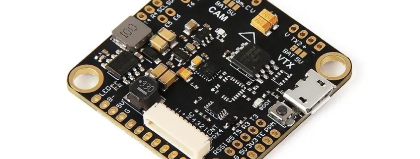
As one of the representatives of modern technology, drones’ circuit boards are the core components for the normal operation of drones. For drone enthusiasts or practitioners, mastering circuit board making skills is crucial. In the process of making a drone circuit board, every detail may affect the final performance and stability.
1. Material selection and preparation
Material quality: Choose high-quality electronic components, wires, solder and other materials to ensure their stable performance and high reliability. Avoid using low-quality materials, which can cause the board to degrade or malfunction.
Material matching: Select suitable components and materials based on the functional requirements and circuit design of the drone. Pay attention to the components’ packaging form, pin spacing and other parameters to ensure that they match the circuit board design.
2. Things to note during the design stage
Layout rationality: When designing a circuit board, fully consider the layout and routing of components. Make sure the components are arranged neatly and compactly, and the wiring is clear and concise. Avoid excessively long traces or cross traces to reduce signal interference and electromagnetic radiation.
Thermal design: Heat dissipation is an important consideration for drone circuit boards. During the design process, heat sinks, fans and other heat dissipation equipment must be reasonably arranged to ensure that the circuit board can maintain good heat dissipation performance during operation.
3. Things to note during the production process
Environmental control: When making circuit boards, pay attention to controlling the temperature, humidity and cleanliness of the working environment. Avoid making circuit boards in a humid and dirty environment to avoid affecting the welding quality and circuit board performance.
Soldering skills: Soldering is one of the key aspects of circuit board production. During the welding process, the welding temperature, time and intensity must be mastered. Avoid excessive welding temperature or too long time, which may cause component damage or poor welding.
Testing and debugging: After completing the soldering, the circuit board needs to be fully tested and debugged. Use professional testing instruments to conduct functional and performance tests on the circuit board to ensure that the circuit board has no hidden faults and has stable performance. During the debugging process, it is necessary to carefully observe the operating status of the circuit board and find and solve problems in time.
4. Safety protection
Anti-static: During the production process, be sure to pay attention to anti-static measures. Use anti-static bracelets, anti-static mats and other tools to prevent static electricity from causing damage to electronic components.
Anti-corrosion: The metal parts of the circuit board are susceptible to corrosion, so pay attention to anti-corrosion measures. Avoid exposing the circuit board to a humid environment for a long time, and clean and maintain the circuit board regularly.
5. Recording and Summary
Production records: During the production process, it is recommended to keep detailed records, including materials used, production processes, problems encountered and solutions, etc. This helps to summarize experiences and lessons and improve production levels.
Problem summary: Problems and difficulties encountered during the production process should be summarized and analyzed in a timely manner. Find out the cause and solution of the problem to avoid repeating mistakes in subsequent production processes.
Drone circuit board production is a job that requires care and patience. Only by mastering the correct production methods and precautions and putting them into practice can we produce a drone circuit board with stable performance and reliable quality.
https://bestpcb-ems.com/wp-content/uploads/2024/07/120.webp.jpg10001000administratorhttps://bestpcb-ems.com/wp-content/uploads/2023/05/logo-pcb2.pngadministrator2024-07-03 07:33:362024-07-03 07:33:42Analysis of drone circuit board production tutorial, things you can’t miss!
The special requirements for automotive circuit boards under IATF16949 certification are very important because these requirements are directly related to the quality and safety of automotive parts. As an integral part of the automotive electronic system, automotive circuit boards must comply with a series of strict standards and specifications to ensure the performance and reliability of the vehicle.
Under IATF16949 certification, the design and manufacturing of automotive circuit boards must meet the special requirements of the automotive industry. This means that the design of automotive circuit boards must take into account the harsh conditions of the automotive working environment, such as high temperature, high humidity, vibration and other factors. At the same time, the material selection and process flow of the circuit board also need to comply with the standards of the automotive industry to ensure that the circuit board has good stability and durability during automobile use.
The quality control and testing requirements for automotive circuit boards are very strict. Manufacturers need to establish a complete quality management system, including full quality control from raw material procurement to finished product delivery. For the testing of automotive circuit boards, in addition to conventional electrical performance tests, special environmental adaptability tests and reliability tests are also required to ensure that the circuit boards can work normally and have long-term reliability in various working environments.
Under IATF16949 certification, the traceability and recording requirements for automotive circuit boards are also very important. Manufacturers need to establish a sound product traceability system to ensure that the production process and usage of each circuit board can be traced. At the same time, manufacturers also need to keep relevant records and documents for audit and verification when necessary.
Under the IATF16949 certification, the special requirements for automotive circuit boards cover all aspects of design, manufacturing, quality control, testing, traceability, etc. Manufacturers must strictly comply with these requirements to ensure the production of high-quality circuit boards that meet automotive industry standards, thereby Improve product competitiveness and gain consumer trust.
https://bestpcb-ems.com/wp-content/uploads/2024/07/119.jpg500888administratorhttps://bestpcb-ems.com/wp-content/uploads/2023/05/logo-pcb2.pngadministrator2024-07-03 07:19:352024-07-03 07:19:40Under IATF16949 certification, how much do you know about the special requirements of automotive circuit boards?