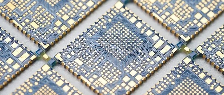
Speed up your circuit design! Understand the characteristics of high-frequency and high-speed PCB!

Circuit design is a job that requires patience and care, as one error may affect the performance and reliability of the entire circuit. In circuit design, high-frequency and high-speed boards are a very important part because its characteristics will greatly affect the performance of the circuit. This article will elaborate on the characteristics of high-frequency and high-speed boards, including signal transmission, EMI suppression, wiring planning and material selection, while also providing some practical tips and suggestions to help speed up your circuit design.

1. Signal transmission

Signal transmission of high-frequency and high-speed boards is one of its most important features. Since high-frequency signals have very high frequencies and short wavelengths, special measures are required to ensure the quality and stability of signal transmission. A common method is to improve the signal-to-noise ratio and anti-interference ability of the signal by using differential signal pairs. In addition, during high-speed signal transmission, signal echo is also a factor that needs to be considered. Because signals travel quickly, echoes can cause signal distortion and performance degradation. In order to reduce echoes, appropriate termination resistors and snubber circuits can be used.

2. EMI suppression

EMI (electromagnetic interference) refers to the electromagnetic radiation generated by electronic equipment and the electromagnetic field interference felt, which can have a negative impact on the performance and stability of circuits. In the design process of high-frequency and high-speed boards, appropriate EMI suppression measures need to be taken. One of the commonly used methods is to reduce the area of the current loop and the path that forms the loop through reasonable layout of circuit traces. This can be accomplished by using ground plans, differential lines, and reducing power and ground current loops.
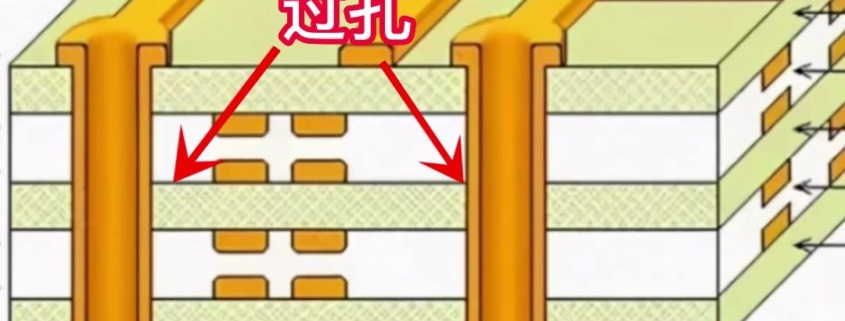
3. Wiring planning

The wiring planning of high-frequency and high-speed boards is a very important step in the design process. When planning wiring, factors such as circuit layout, wiring, power lines, and ground wires need to be considered. One common approach is to use different layers for routing. For example, you can use the inner layer for routing power and ground lines, and the outer layer for routing data lines. Through this method, the length and intersection of traces can be reduced, and signal distortion and noise interference can be reduced.

4. Material selection

The material selection of high-frequency and high-speed boards also affects the performance and reliability of the circuit. For example, different dielectric constants and dielectric losses affect the speed and transmission quality of signals. Therefore, when selecting materials, factors such as the dielectric constant, dielectric loss, thermal expansion coefficient, and thermal conductivity of the board need to be considered. At the same time, factors such as the cost and reliability of materials also need to be considered.

High-frequency and high-speed boards are a very important part of circuit design and require special attention to factors such as signal transmission, EMI suppression, wiring planning, and material selection. By using the appropriate techniques and measures, you can improve circuit performance and reliability and speed up your circuit design.

What is the function of PCB half hole?

1、 Strengthening connections

The connectivity between electronic components is the foundation of circuit boards. In traditional circuit board manufacturing, electronic components are usually soldered onto the surface of the circuit board, and the connection method is relatively simple, which is prone to poor connectivity or virtual soldering. The use of PCB half hole technology can improve the connectivity between electronic components, making the performance of circuit boards more stable and reliable. In PCB half hole technology, electronic components are not only connected to the surface of the circuit board, but also pass through the PCB half hole and penetrate into another layer of the circuit board. In this way, the connectivity between electronic components becomes tighter, making it easier to meet the requirements of circuit board designers and improve the performance and reliability of circuit boards.

2、 Improve signal quality

The quality of the signal has a significant impact on the performance of the circuit board. In traditional circuit board manufacturing, signal lines are often affected by wiring or environmental factors, which can easily lead to signal crosstalk or signal loss. By using PCB half hole technology, these issues can be effectively improved. The signal line can pass through the PCB half hole and penetrate into another layer of the circuit board, thereby avoiding interference from wiring or environmental factors on the signal line. Meanwhile, due to the tighter connection between signal lines and electronic components, the quality of signal transmission will also be more stable, thereby improving the operational efficiency and reliability of the circuit board.

3、 Improve mechanical strength

Mechanical strength is a very important indicator in circuit board manufacturing. In traditional circuit board manufacturing, due to loose connections between electronic components and circuit boards, the mechanical strength of circuit boards is low, making them prone to bending or breaking. By using PCB half hole technology, the mechanical strength of the circuit board can be effectively improved. Electronic components are not only connected to the surface of the circuit board, but also penetrate through PCB half holes and penetrate into another layer of the circuit board. This design can make the connections between electronic components tighter, thereby enhancing the mechanical strength of the circuit board, reducing the probability of breakage, and improving the durability of the circuit board.

4、 Implement a multi-layer board structure

The multi-layer board structure is widely used in the manufacturing of modern circuit boards. It can greatly reduce the size and weight of the circuit board, while improving its performance and reliability. By using PCB half hole technology, a multi-layer board structure can be achieved. Electronic components can penetrate through PCB half holes and penetrate into another layer of the circuit board. In this way, the circuit board can be divided into multiple layers, achieving a multi-layer board structure. Compared with traditional multi-layer board manufacturing, PCB half hole technology not only makes multi-layer boards more precise, but also saves costs and time, improving manufacturing efficiency.

PCB half hole technology is an important technology in modern circuit board manufacturing. It plays an important role in strengthening connections, improving signal quality, enhancing mechanical strength, and achieving a multi-layer board structure. The use of PCB half hole technology to manufacture circuit boards is more precise and efficient, while also improving the performance and reliability of the circuit board. With the continuous development of electronic technology, PCB half hole technology will be further improved and promoted, bringing more innovation and development to circuit board manufacturing.

Which wiring form is better for PCB design?

In PCB design, adopting appropriate wiring forms has a significant impact on the performance and reliability of the circuit. The following are several common wiring forms, each with its own advantages. Choosing the appropriate form based on specific design requirements will be more conducive to improving circuit performance and reliability.

1. Straight line routing: Straight line routing is the simplest and most common form of routing. It has the advantage of being direct and fast, which can reduce the delay of signal transmission. In circuit design, there are often signal lines that must be connected in a straight line, so using straight line routing can better meet this requirement.

2. 45 degree bend wiring: When it is necessary to introduce or lead the signal line into or out of the board, using a 45 degree bend wiring can reduce the reflection and interference of the signal line. Compared to right angle bending, 45 degree angle bending can better maintain the integrity of the signal.

3. Arc routing: Arc routing can reduce the radiation and crosstalk of signal lines, especially for high-frequency signals. If there are high-frequency signal lines in the design, using arc routing can reduce signal loss and distortion.

4. Node cross routing: In design, it is common to encounter situations where cross signals need to be connected. When cross routing nodes, attention should be paid to the distance between signal lines to prevent signal crosstalk. Interlayer routing, ground cutting, and other methods can be used to reduce signal interference.

5. Hard and flexible wiring: Hard and flexible wiring refers to signal transmission achieved through interlayer connections. It can improve the flexibility and reliability of design. Hard and flexible wiring is widely used in complex high-density circuit design, multi-layer board design, and so on.

6. Top/bottom wiring: In multi-layer board design, the top and bottom wiring can be used for shorter signal transmission paths, thereby reducing interlayer perforation and delay. At the same time, the top/bottom wiring can provide better shielding effect and reduce signal interference.

Although several common wiring forms are listed above, multiple factors need to be considered in actual design to choose the appropriate form. For example, the frequency characteristics of circuits, noise tolerance, power consumption requirements, and process constraints. When wiring, attention should also be paid to the separation between the signal, power supply, and ground wire, and the reasonable use of ground wire shielding technology.

In short, choosing the appropriate wiring form is crucial for the performance and reliability of the circuit. Based on specific design requirements and circuit characteristics, designers should comprehensively consider various factors and choose the optimal wiring form to optimize circuit design.

What are the protective measures and maintenance methods for PCB multi-layer circuit boards?

(1). Environmental protection

1. Keep the board surface dry: Excessive humidity can cause electrochemical reactions, oxidation and corrosion in multi-layer board circuits, and even cause short circuits in severe cases. Therefore, the environmental requirements for using PCB multi-layer circuit boards are relatively high, so try to keep the environment dry.

2. Pay attention to dust prevention: Dust and dirt are one of the main culprits that cause multi-layer PCB circuit board failures. Once they enter the circuit board, they will cause problems such as short circuit, discharge, leakage, etc. In serious cases, they may damage the PCB circuit board.

3. Avoid mechanical damage: Do not collide or scratch the surface of the multi-layer circuit board to avoid breaking the internal circuits and causing failure. At the same time, it is also necessary to avoid excessive force and pressure to prevent flexural damage to the board.

(2). Manufacturing process

1. Strengthen design protection: During the design stage of PCB multi-layer circuit boards, attention should be paid to preventing possible problems and relevant protection measures should be set in advance. For example, divide high-voltage and high-current lines and low-voltage and low-current lines into different levels, and try to avoid running the lines in the same way or intersecting.

2. Strict quality control: Detailed quality control is required for each link during the manufacturing process. For example, operations in manufacturing processes such as drilling, crimping, and immersion metal need to be standardized to avoid human errors.

(3). Transportation and installation

1. Prevent collisions: During the transportation of PCB multi-layer circuit boards, it is necessary to prevent them from being damaged by collisions with other hardware or products. Therefore, circuit boards need to be installed in special packaging boxes for transportation to avoid being affected by external forces.

2. Note on braking: When transporting multi-layer circuit boards, it is necessary to brake and slow down to avoid problems such as friction and heat caused by free sliding between the boards, resulting in line deformation and other problems.

(4). Daily maintenance

1. Regular dust removal: In order to ensure the good working condition of the circuit board, regular dust removal is required to avoid the harm of dust to the circuit board. At the same time, you can also check the appearance of the circuit board for scratches or damage.

2. Replace capacitors regularly: Capacitors are one of the more easily damaged components in multi-layer PCB circuit boards. Once the service life expires or is affected by external factors, when problems occur, they should be replaced in time.

3. Keep dry: The working environment of multi-layer circuit boards needs to be dry. Avoid keeping circuit boards in a humid environment during daily maintenance. Pay attention to moisture-proofing during the rainy season.

When using PCB multi-layer circuit boards, you need to pay attention to protection and maintenance. Starting from four aspects: environmental protection, manufacturing technology, transportation and installation, and daily maintenance, the protective measures and maintenance methods of PCB multi-layer circuit boards are elaborated in detail. These measures play an important role in ensuring the normal operation of PCB multi-layer circuit boards during use, and are also of great significance in improving the reliability and service life of electronic products.

What are the benefits of Immersion Gold PCB?

1. Corrosion resistance

Immersion gold PCB has excellent corrosion resistance. Its surface metal coating can effectively prevent the PCB board from being corroded by the external environment. Compared with other surface treatment processes, immersion gold PCB can better resist oxidation, sulfuration and chemical corrosion, thereby extending the service life of the circuit board.

2. Reliability

Immersion gold PCBs are widely used in electronic product manufacturing, mainly because of its reliability. The immersion gold layer has good flatness and smoothness and can provide a good welding surface. This makes the welding process more stable and reduces the risk of poor welding. In addition, immersion gold PCB can also provide good signal transmission performance, reduce signal loss and interference, and improve circuit reliability.

3. Weldability

Immersion gold PCB has good solderability. The immersion gold layer has good wettability and solderability, and can be well combined with solder. This makes the welding process easier and more stable, greatly improving welding efficiency. At the same time, the flatness and smoothness of the immersion gold layer also help reduce welding defects and improve welding quality.

4. Conductivity

Immersion gold PCB has excellent conductive properties. The immersed gold layer has the characteristics of low resistance and low reflectivity, which can provide low noise and stable signal transmission. This is very important for high frequency and high speed circuits. In addition, the immersion gold layer also has good current carrying capacity and can meet the needs of various circuit boards.

Immersion gold PCB has many advantages such as corrosion resistance, reliability, weldability and conductivity, so it plays an important role in electronic product manufacturing, providing a stable soldering surface and reliable signal transmission. With the continuous development of electronic products, the application prospects of immersion gold PCB will be broader.

What is via hole?

Via hole is one of the important components of multi-layer PCB, and the cost of drilling usually accounts for 30% to 40% of the PCB board manufacturing cost. Simply put, every hole on the PCB can be called a via. From a functional point of view, vias can be divided into two categories: one is used for electrical connections between layers; the other is used for fixing or positioning devices. From a process perspective, these vias are generally divided into three categories, namely blind vias, buried vias and through vias. Blind holes are located on the top and bottom surfaces of the printed circuit board and have a certain depth. They are used to connect the surface circuits and the inner circuits below. The depth of the holes usually does not exceed a certain ratio (aperture). Buried vias refer to connection holes located on the inner layer of a printed circuit board and do not extend to the surface of the circuit board. The above two types of holes are located in the inner layer of the circuit board. They are completed using the through-hole forming process before lamination. During the via-hole formation process, several inner layers may be overlapped.

The third type is called a through hole, which passes through the entire circuit board and can be used to implement internal interconnections or as mounting positioning holes for components. Because through holes are easier to implement in technology and have lower costs, most printed circuit boards use them instead of the other two via holes. The following via holes are considered as through holes unless otherwise specified.

From a design point of view, a via hole mainly consists of two parts, one is the drill hole in the middle, and the other is the pad area around the drill hole. The size of these two parts determines the size of the via. Obviously, when designing high-speed, high-density PCBs, designers always hope that the via holes should be as small as possible, so that more wiring space can be left on the board. In addition, the smaller the via holes, the smaller their own parasitic capacitance will be. The smaller it is, the more suitable it is for high-speed circuits. However, the reduction in hole size also brings about an increase in cost, and the size of the via hole cannot be reduced indefinitely. It is limited by process technologies such as drilling (drill) and electroplating (plating): the smaller the hole, the harder it is to drill. The longer the hole takes, the easier it is to deviate from the center; and when the depth of the hole exceeds 6 times the drill diameter, there is no guarantee that the hole wall will be evenly plated with copper. For example, if the thickness (through hole depth) of a normal 6-layer PCB board is 50 Mil, then under general conditions, the drilling diameter that the PCB manufacturer can provide can only reach 8 Mil. With the development of laser drilling technology, the size of drilled holes can also become smaller and smaller. Generally, vias with a diameter of less than or equal to 6 Mils are called microvias. Microvias are often used in HDI (High Density Interconnect Structure) design. Microvia technology allows vias to be drilled directly on the pad (Via-in-pad), which greatly improves circuit performance and saves wiring space.

What does high speed pcb mean?

High-speed PCB boards, as the name suggests, refer to PCB boards used in high-speed circuits, generally used in communications, computers, military and other fields. High-speed PCB board is a widely used electronic component that has excellent performance in high frequency, high-speed transmission, signal integrity, etc. So what exactly does high-speed PCB mean? In fact, it means that the signal transmission rate in high-speed circuits is relatively fast, and special design techniques and materials are required to ensure the stability and reliability of the signal.

In high-speed PCB design, the signal transmission rate and attenuation need to be considered. In order to ensure the stability of the signal, short and thick wires need to be used to reduce signal reflection and interference. At the same time, a laminate design is also needed to separate the ground and power planes to avoid interference and crosstalk.

In terms of material selection, high-speed PCB needs to use low dielectric constant materials, such as PTFE, FR-4, etc. This can reduce signal transmission delay and loss, and improve signal transmission rate and quality.

When wiring high-speed PCB, you also need to pay attention to signal matching and impedance control. Through reasonable wiring methods and impedance control, signal reflection and loss can be effectively reduced and signal stability and reliability improved.

High-speed PCB boards play an important role in the field of modern electronics and require special design techniques and materials to ensure signal stability and reliability.

What is the use of pcb impedance board?

PCB impedance board is an indispensable part of modern electronic manufacturing. It plays an important role in circuit wiring, signal integrity, power consumption control and EMI anti-interference. By controlling the impedance value and optimizing the circuit design, the signal transmission quality can be improved, power consumption can be reduced, and the reliability and anti-interference ability of the circuit can be improved.

1. Definition and basic principles of PCB impedance board

PCB (printed circuit board) impedance board refers to a printed circuit board that uses specific materials and technologies to achieve specific impedance values when designing and manufacturing electronic equipment. Impedance value refers to the resistance that current encounters when it travels in a circuit. PCB impedance boards achieve specific impedance values by controlling parameters such as line width, spacing, layer spacing, lead length, and ground holes between layers.

2. The use of circuit wiring

In high-frequency circuits, the signal transmission speed is very fast. To ensure the integrity of the signal, it is necessary to use an impedance matching circuit. The PCB impedance board can ensure that the signal transmission speed on the circuit board is consistent and avoid signal distortion and attenuation. At the same time, the impedance board can also reduce signal crosstalk and improve signal reliability.

3. The use of signal integrity

PCB impedance board can effectively reduce signal reflection and interference and improve signal integrity. In high-speed signal transmission, if the signal reflection amplitude is too large, it will cause signal distortion and increase power consumption. Impedance boards can reduce signal reflection and interference and improve signal transmission quality by controlling circuit wiring and adjusting circuit parameters.

4. The use of power consumption control

When the impedance matching of the circuit is not guaranteed, current will be reflected in the circuit, which will lead to energy loss and increase in power consumption. PCB impedance board can reduce signal reflection and interference, thereby reducing power consumption. In large-scale integrated circuits, power consumption control is very important, and the impedance board plays an important role in power consumption control.

5. The use of EMI anti-interference

Electromagnetic interference (EMI) is a serious problem in modern electronic equipment. The PCB impedance board can suppress signal radiation and interference and reduce the impact of electromagnetic waves on other electronic equipment. At the same time, the impedance board can also prevent external electromagnetic signals from entering the circuit and improve the anti-interference ability of the circuit.

What are the functions of Rigid-Flex circuit boards?

The combination of Rigid-Flex circuit boards refers to the combination of software and hardware in circuit board design to achieve more efficient and stable circuit functions.

1. Improve production efficiency

The design of the Rigid-Flex circuit board can reduce the wiring length while making the connections between circuit components closer, thereby reducing electromagnetic interference and signal loss. In addition, the excellent design of hard-soft circuit boards can shorten the production cycle, reduce manual operations and error rates, and improve production efficiency. Therefore, the design of Rigid-Flex circuit boards can help improve production efficiency and create greater economic benefits for enterprises.

2. Improve product reliability

The design of the Rigid-Flex circuit board can reduce the contact resistance and inductance between circuit components, thereby improving the stability and reliability of the circuit. In addition, the design of the Rigid-Flex circuit board can reduce the welding and plugging on the circuit board, thereby reducing the impact of human factors and improving product reliability. Therefore, the design of  Rigid-Flex circuit boards can help improve product reliability and establish a good brand image for the company.

3. Reduce costs

The design of a  Rigid-Flex circuit board can make the connection between circuit components closer, thereby reducing the area of the circuit board and the amount of material used. In addition, the design of Rigid-Flex circuit boards can reduce the production cycle and manual operations, thereby reducing the company’s production costs. Therefore, the design of circuit boards that combine Rigid-Flex circuit boards can help reduce corporate costs and improve corporate competitiveness.

4. Enhance product safety

The design of a  Rigid-Flex circuit board can reduce the contact resistance and inductance between circuit components, thereby reducing the failure rate and safety hazards of the circuit board. In addition, the design of the Rigid-Flex circuit board can enhance the product’s anti-interference ability and lightning protection ability, thereby enhancing product safety. Therefore, the design of circuit boards that combine Rigid-Flex circuit boards can help enhance product safety and protect enterprises.

The role of  Rigid-Flex circuit boards is multi-faceted. It can improve production efficiency, improve product reliability, reduce costs, and enhance product safety. With the continuous development of science and technology and the continuous demand of the market, the application of  Rigid-Flex circuit boards will become more and more widespread. Therefore, companies should strengthen the research and application of  Rigid-Flex circuit boards to improve product quality and competitiveness.

What are the advantages of thick copper PCB?

Thick copper PCB is a high-performance PCB that is widely used in high-power electronic devices due to its unique performance and characteristics.

1、 Good thermal conductivity
The copper layer thickness of thick copper PCBs is relatively large, usually reaching 10oz in the inner layer and 6oz in the outer layer, which is much thicker than the 1oz thickness of conventional PCBs. The increase in copper layer thickness significantly improves the thermal conductivity of the PCB board, reduces line resistance, lowers component temperature, and thus improves the reliability, stability, and lifespan of the circuit.

2、 Excellent current carrying capacity
The increase in the thickness of the inner and outer layers of the thick copper plate PCB effectively increases the conductive area of the circuit and improves its ability to carry current. In addition, the thick copper PCB also uses distributed inductance technology and blind buried hole technology, greatly reducing the self inductance of the current and enabling it to withstand higher currents. Therefore, in the design of high-power electronic devices, thick copper plate PCBs have unique advantages.

3、 Excellent corrosion resistance

The copper layer of thick copper PCB not only has a large thickness, but also uses pure copper material. This material can effectively improve the corrosion resistance of PCB boards and extend their service life. In addition, in terms of sputtering etching technology for copper layers, the process of thick copper PCB has been highly mature, which can effectively avoid circuit problems caused by uneven etching.

4、 Better mechanical performance
Due to the thicker copper layer of thick copper PCB, the thickness of the entire board is also larger. Therefore, the PCB has better mechanical strength and stiffness, which can better protect circuits in complex physical environments. At the same time, thick copper PCBs can also be stacked in multiple layers according to practical applications, making the overall structure more compact and sturdy.

With the continuous development of electronic products, thick copper PCBs will have more and more widespread applications.