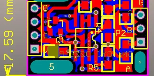
Is PCB board size marking really that important?

PCB board dimensioning plays a vital role in circuit design and production. It not only ensures the normal operation of the circuit board, but also improves production efficiency and reduces costs. This article will elaborate on the importance of PCB board dimension marking from four aspects, including design specifications, production process, assembly process and reliability testing.

1. Design specifications

PCB board size marking plays an important role in the early stage of circuit design. Reasonable dimensioning can ensure the stability of the connection and installation of the circuit board and external devices, and avoid connection problems and poor signal transmission caused by inappropriate dimensions. In addition, accurate dimensioning can also help designers better control the size and shape of circuit boards during layout to adapt to different application scenarios.

2. Production process

PCB board size marking also has an important impact on the circuit board production process. Reasonable dimensioning can help manufacturers accurately cut circuit boards and avoid waste and repeated processing caused by size discrepancies. In addition, dimensional markings can also guide production personnel in drilling, mounting and other process operations, improving production efficiency and product quality.

3. Assembly process

PCB board size marking also plays a vital role in the circuit board assembly process. Accurate dimensioning can help assemblers install components correctly and avoid problems such as component misalignment and poor welding caused by size discrepancies. In addition, dimensional markings can also guide assembly personnel in welding, testing and other process operations, improving assembly efficiency and product quality.

4. Reliability test

PCB board size marking is also very important for circuit board reliability testing. Reasonable dimensioning can help testers install test equipment accurately and ensure test accuracy and reliability. In addition, dimensional markings can also guide testers to perform operations such as signal testing and temperature testing, improving test efficiency and reliability of results.

From the four aspects of design specifications, production process, assembly process and reliability testing, the importance of PCB board size marking cannot be ignored. Reasonable dimensioning can ensure the normal operation of circuit boards and improve production efficiency and product quality. Therefore, in circuit design and production, we should pay attention to the dimension marking of PCB boards and rationally use marking technology to ensure the stability and reliability of the circuit board.

Enhance product performance! The strong competitive advantage brought by multi-layer PCB lamination process!

As technology continues to advance, the demand for electronic products is also growing. In order to meet consumer requirements for higher performance and smaller size, the multi-layer PCB lamination process has become a key link in the design of modern electronic products.

Multi-layer PCB lamination process can provide higher circuit density. Compared with traditional single-layer circuit boards, multi-layer PCBs can accommodate more electronic components and connection lines, thereby achieving more complex functional integration. This is critical for modern electronics, which often require more functionality and performance in a limited space.

The multi-layer PCB lamination process can also improve the stability and reliability of the circuit. Since the multi-layer PCB adopts a stacked design, the connections between electronic components are closer, reducing interference and loss in signal transmission. In addition, multi-layer PCBs also have better anti-interference performance and can effectively resist external electromagnetic interference and noise. These characteristics make multi-layer PCBs perform well in application fields such as high frequency and high-speed transmission.

In addition, the multi-layer PCB lamination process can also improve the heat dissipation performance of the product. As the power consumption of electronic products increases, heat dissipation issues have become an important factor restricting product performance. The stacking design of multi-layer PCB can effectively improve the heat dissipation effect. Through reasonable thermal conduction design and heat dissipation channels, heat is quickly conducted to the external environment and the normal operating temperature of electronic components is maintained, thereby improving the stability and life of the product.

The multi-layer PCB lamination process can also simplify the product manufacturing process. Compared with using multiple single-layer circuit boards for assembly, multi-layer PCBs can directly weld electronic components to different levels of circuit boards, reducing the use of connecting wires, simplifying the assembly process, and improving production efficiency. This is especially important for large-scale production and fast delivery requirements.

In the electronics industry, mastering the design and manufacturing technology of multi-layer PCB lamination process will bring greater market competitiveness to enterprises. Therefore, we should pay attention to the application and development of multi-layer PCB lamination technology and continuously promote the enhancement of product performance to meet users’ needs for high-quality electronic products.

What is copper-clad? Grid copper coating or solid copper coating?

1. What is copper coating?

The so-called copper pouring is to use the idle space on the circuit board as the reference plane and then fill it with solid copper. These copper areas are also called copper filling.

The significance of copper coating is to reduce the impedance of the ground wire and improve the anti-interference ability; reduce the voltage drop and improve the power efficiency; connecting to the ground wire can also reduce the loop area.

Also for the purpose of keeping the PCB from deforming as much as possible during welding, most PCB manufacturers will also require PCB designers to fill the open areas of the PCB with copper or grid-like ground wires. If the copper is not handled properly, it will The gain outweighs the loss. Does copper coating have “more pros than cons” or “does more cons than pros”? Everyone knows that at high frequencies, the distributed capacitance of the wiring on the printed circuit board will work. When the length is greater than 1/20 of the corresponding wavelength of the noise frequency, the antenna effect will occur, and the noise will be emitted outward through the wiring. If there is poorly grounded copper in the PCB, the copper becomes a tool for transmitting noise.

Therefore, in high-frequency circuits, do not think that the ground wire is connected to the ground somewhere. This is the “ground wire”. You must drill holes in the wiring with a spacing of less than λ/20, and connect it to the ground. The ground plane of the shelf is “well grounded”. If the copper coating is handled properly, the copper coating not only increases the current, but also plays the dual role of shielding interference.

2. Two forms of copper pouring

There are generally two basic methods of copper pouring, namely large-area copper pouring and grid copper pouring. People often ask whether it is better to pour copper pouring over a large area or with grid copper pouring. It is difficult to generalize.

why? Covering a large area with copper has the dual functions of increasing current and shielding. However, if a large area of copper is covered with wave soldering, the board may warp or even blister. Therefore, when covering a large area with copper, several grooves are usually opened to alleviate blistering of the copper foil.

Pure grid copper coating mainly has a shielding effect, and the effect of increasing current is reduced. From the perspective of heat dissipation, the grid is beneficial (it reduces the heating surface of copper) and plays a certain role in electromagnetic shielding. Especially for circuits such as touch, as shown below: It should be pointed out that the grid is composed of traces in staggered directions. We know that for circuits, the width of the traces has its influence on the operating frequency of the circuit board. The corresponding “electrical length” (can be obtained by dividing the actual size by the digital frequency corresponding to the operating frequency, see relevant books for details).

When the operating frequency is not very high, perhaps the role of the grid lines is not very obvious. Once the electrical length matches the operating frequency, it is very bad. You will find that the circuit cannot work properly at all, and interference is being emitted everywhere. signal of.

The suggestion is to choose based on the working conditions of the designed circuit board, and don’t stick to one thing. Therefore, high-frequency circuits have multi-purpose grids that require high interference resistance, and low-frequency circuits have high-current circuits and other circuits that commonly use complete copper laying.

What are the requirements and precautions for PCB silkscreen design?

1. Silkscreen design requirements

The ratio of character height to character width of silkscreen characters is generally required to be ≥6:1. There are three common font sizes: among them, when the board density is relatively high, 4/25mil characters (No. 1) are commonly used; when the density is normal, 5/ 30mil characters (No. 2); when the board is relatively loose, 6/45mil characters (No. 3) are recommended; usually the base copper thickness of the surface layer also has corresponding requirements for the silk screen width, base copper <1OZ, limit value ≥4mil, optimization value ≥6mil; When the base copper thickness is 1OZ, 5/30mil characters are preferred; when the base copper thickness is 2OZ, 6/45mil characters are preferred.

2. Requirements for adding PCB silkscreen printing

1. Placement: Generally speaking, when placing the silk screen of resistors, capacitors, tubes and other devices, do not use four directions. This will make it very tiring to look at the silkscreen during debugging, maintenance and welding ( How many directions does the board need to turn).

2. Try not to punch the via holes on the silk screen.

3. Do not press the silk screen on high-speed signal lines (such as clock lines, etc.): For high-speed signal lines on the top or bottom layer, because such signal lines can be regarded as microstrip lines.

4. The reading direction of the silk screen should be consistent with the usage direction. The reading direction of the silkscreen should be consistent with the usage direction of the chip. This is mainly to reduce the probability of reverse soldering when welding.

5. The pin number must be clearly marked on the silkscreen.

6. Silkscreen printing for special packages: For special packages such as BGA and QFN, the size of the silk screen must be exactly the same as the size of the chip.

7. Silkscreen printing of the mounting holes: The silkscreen printing of the screws is added near the mounting holes, and the length and total number of screws are also marked to facilitate installation.

3. Precautions for silkscreen design

1. The silkscreen line width on the board should be ≥ 4 mil, and avoid the screen printing line width of components being 0.

2. The distance between the silkscreen and the pads: Do not cover the soldering points on the board with the silkscreen, such as the pads of SMD devices and the through holes of plug-ins. The silkscreen is an insulating material. Once it is applied to the pads, it will cause poor welding; do not cover the test points on the board. , mark points, etc.; it is usually required to maintain a 6mil spacing.

3. The spacing between silkscreens: maintain 6 mil. Overlapping between silkscreens is acceptable. Once the overlap causes unrecognizability, it needs to be adjusted away.

4. Silk screen printing direction: The arrangement of silkscreen strings should follow the principle of from left to right or bottom to top when looking at the screen.

5. Placement of device reference numbers: The device reference numbers should correspond to the devices one-to-one, and the order cannot be reversed or changed. When the device density is relatively high, the method of drawing out labels or symbol markings can be used to place the reference numbers on other parts of the board. Wherever there is space.

6. The component polarity markings and “1” pin markings must be placed correctly and clearly.

7. When introducing annotations or symbol annotations, the added silkscreen and characters should be placed on the silkscreen layer of Board Geometry.

The added board name and version number silkscreen is also placed on the silkscreen layer of Board Geometry.

8. The device tag cannot be placed inside the device body or outside the board frame.

9. When the board density is relatively high and there is really no space to place the tags, you can discuss with the customer not to use the tags, but an assembly drawing is required to facilitate device installation and inspection.

10. When the customer requires copper characters to be written on the top and bottom layers, the line width of the copper characters: HOZ base copper – the character width is more than 8 mil and the height is more than 45 mil; 1OZ base copper – the character width is more than 10 mil and the height is more than 50 mil. At the same time, it is necessary to open the solder mask window so that the copper characters on the produced board will be brighter.

How to design PCB safety spacing?

There are many places where safety distances need to be considered in PCB design. Here, they are temporarily classified into two categories: one is electrical-related safety distances, and the other is non-electrical-related safety distances.

1. Electrical related safety distances

1. Spacing between wires

As far as the processing capabilities of mainstream PCB manufacturers are concerned, the distance between wires must not be less than 4mil. Line spacing is also the distance from line to line and line to pad. From a production perspective, the bigger the better if conditions permit, and 10mil is more common.

2. Pad aperture and pad width

In terms of the processing capabilities of mainstream PCB manufacturers, the pad aperture should not be less than 0.2mm if mechanical drilling is used, and should not be less than 4mil if laser drilling is used. The aperture tolerance varies slightly depending on the board material. It can generally be controlled within 0.05mm, and the pad width must not be less than 0.2mm.

3. The spacing between pads

In terms of the processing capabilities of mainstream PCB manufacturers, the distance between pads must not be less than 0.2mm.

4. The distance between the copper sheet and the edge of the board

The distance between the charged copper sheet and the edge of the PCB board shall not be less than 0.3mm. As shown in the figure above, set this spacing rule on the Design-Rules-Board outline page.

If a large area of copper is laid, there is usually a shrinkage distance from the edge of the board, which is generally set to 20mil. In the PCB design and manufacturing industry, generally, engineers often lay large areas of copper out of mechanical considerations for the finished circuit board, or to avoid curling or electrical short circuits due to copper being exposed on the edge of the board. The block is retracted 20mil relative to the edge of the board instead of spreading the copper all the way to the edge of the board. There are many ways to deal with this copper shrinkage, such as drawing a keepout layer on the edge of the board, and then setting the distance between the copper laying and the keepout. Here is a simple method, which is to set different safety distances for copper-laying objects. For example, the safety distance for the entire board is set to 10mil, and the copper-laying setting is 20mil. This can achieve the effect of shrinking the edge of the board by 20mil, and at the same time Eliminates dead copper that may appear within the device.

2. Non-electrical related safety distances

1. Character width, height and spacing

No changes can be made to the text film during processing, except that the character line widths with D-CODE less than 0.22mm (8.66mil) are thickened to 0.22mm, that is, the character line width L=0.22mm (8.66mil), and the entire character The width = W1.0mm, the height of the entire character H = 1.2mm, and the spacing between characters D = 0.2mm. When the text is smaller than the above standards, it will be blurry when printed.

2. Via-to-via spacing (hole edge to hole edge)

The distance from via (VIA) to via (hole edge to hole edge) is greater than 8mil.

3. Distance from silk screen to solder pad

Screen printing is not allowed to cover the soldering pads. Because if the silk screen covers the soldering pad, tin will not be applied to the silk screen area during tin application, which will affect the mounting of components. Generally, board manufacturers require a spacing of 8mil. If the PCB board area is really limited, a 4mil spacing is barely acceptable. If the silk screen accidentally covers the pad during design, the board manufacturer will automatically remove the silk screen left on the pad during manufacturing to ensure that the pad is tinned.

Of course, the specific situation should be analyzed in detail during design. Sometimes the silk screen is deliberately placed close to the pads, because when the two pads are very close, the silk screen in the middle can effectively prevent the solder connection from short-circuiting during soldering. This situation is another matter.

4. 3D height and horizontal spacing on the mechanical structure

When mounting components on the PCB, it is necessary to consider whether they will conflict with other mechanical structures in the horizontal direction and spatial height. Therefore, when designing, it is necessary to fully consider the compatibility between components, between the finished PCB and the product shell, and the spatial structure, and reserve a safe distance for each target object to ensure that there is no spatial conflict.

Connect the world! Explore the application of fpc pcb design in the communication field!

In recent years, with the rapid development of communication technology, the application of FPC PCB design in the communication field has attracted more and more attention. FPC PCB is a circuit board made of flexible substrate. It is thin, flexible and widely used in electronic products such as mobile phones, tablets and smart wearable devices. In the vast communication network connecting the world, FPC PCB board design plays an important role.

The application of FPC PCB design in the communication field has greatly improved the flexibility and reliability of the equipment. Compared with traditional rigid circuit boards, the flexibility of  flexible boards allows electronic devices to better adapt to various shapes and sizes. Whether it is a curved screen or a foldable display, FPC PCB can meet its complex wiring requirements, making the device thinner, lighter and more portable. At the same time, the reliability of FPC PCB has also been greatly improved. It has good earthquake resistance and tensile resistance, which can effectively reduce damage caused by external forces and extend the service life of equipment.

The application of FPC PCB design in the communication field expands the functions and performance of the device. Through flexible wiring and multi-layer structure design, FPC PCB can accommodate more electronic components and achieve more complex circuit connections. In communication equipment, the application of FPC PCB makes the data transmission between various modules more efficient and stable, improving the response speed and data processing capabilities of the equipment. At the same time, the FPC PCB can also integrate functional modules such as antennas and sensors, which further enhances the functionality of the device and meets users’ needs for diverse functions.

In addition, the application of FPC PCB design in the communication field also brings new opportunities for innovation in communication technology. With the advent of the 5G era, communication equipment has increasingly higher requirements for high frequency and high speed. The FPC PCB has the advantages of good high-frequency characteristics and low transmission loss, which can meet the needs of high-speed data transmission and provide support for the development of 5G communication technology. At the same time, FPC PCB can also be used in emerging fields such as flexible display and virtual reality, providing a broader space for technological innovation.

The application of FPC PCB design in the communication field is constantly promoting the development of communication technology. Its flexibility, reliability, and improvements in functionality and performance enable communication devices to better connect the world and meet user needs. With the continuous advancement of technology, I believe that the application of FPC PCB design in the communication field will bring more innovations and breakthroughs, bringing a better future to our communication world!

What is the difference between impedance PCB and non-impedance PCB?

PCB board impedance control technology is an important link in PCB production. Impedance-controlled PCB boards can ensure the quality of signal transmission, but the cost will be relatively high. Non-impedance boards are relatively cheap, but in high-speed signal transmission environments, the signal transmission quality may decrease.

1. Definition and principles of impedance PCB and non-impedance PCB

Impedance control technology refers to controlling the impedance of electronic signals through the wiring design and manufacturing process of PCB boards to minimize distortion and reflection of signals during transmission. The impedance board uses special materials and manufacturing processes to control parameters such as line width, distance, load, etc. to ensure the stability and accuracy of signal transmission. Non-impedance boards use general PCB manufacturing processes and do not pay attention to signal impedance control.

2. Advantages and Disadvantages of  impedance PCB and non-impedance PCB

The main advantage of impedance plates is the high quality of signal transmission. The impedance-controlled PCB board can reduce signal distortion and reflection, and can also reduce signal interference and crosstalk, ensure that circuit noise is small, and improve signal transmission accuracy and stability. However, the cost of impedance control is relatively high, and the material and process requirements for PCB boards are also relatively high. In some special high-frequency and high-speed environments, impedance control may not fully meet the requirements. The main advantages of non-impedance boards are low production cost, simple production process and short manufacturing cycle. For some occasions where the transmission rate is not high and the circuit is simple, non-impedance boards can also meet the requirements. However, in some high-speed and high-frequency environments, non-impedance boards are prone to problems such as signal distortion, crosstalk, and noise, which will have a certain impact on the working stability and reliability of the circuit.

3. Applications of impedance PCB and non-impedance PCB

Impedance control technology is often used in high-speed signal transmission, high-frequency circuits, analog circuits and other fields. Usually in the design of high-speed AD, DA converters and high-speed digital signal processors, PCB boards using impedance control technology are required to ensure signal accuracy and stability. Non-impedance boards are usually used in some low-speed and low-frequency circuit designs, such as LED light bars, home appliance control boards, etc.

4. Manufacturing requirements and methods of impedance PCB and non-impedance PCB

The production of impedance-controlled PCB boards is highly demanding, requiring the use of high-precision manufacturing equipment and fine control of the materials and processes of the PCB boards. This can be achieved by using some high-impedance control design software and manufacturing processes. For example, during the design process, the upper and lower copper foils can be wired together to form a differential impedance. Use high dielectric constant dielectrics with controlled impedance greater than 1 such as FR4, ROGERS, etc. Non-impedance boards are relatively simple to make, and the process and material selection are also more flexible.

Impedance PCB and non-impedance PCB are suitable for different circuit design needs. Impedance PCB can ensure the quality of signal transmission in high-speed and high-frequency circuits, but the cost is relatively high. Non-impedance boards are suitable for the design of some low-frequency and low-speed circuits and have lower costs. Therefore, when selecting PCB board type, you need to make a reasonable choice based on the specific application environment and circuit design requirements.

What is the difference between high-frequency circuit boards and ordinary circuit boards? Comprehensive analysis of advantages and disadvantages!

High-frequency circuit boards have higher operating frequencies and lower signal distortion rates, but their manufacturing costs are higher and manufacturing is more difficult. Ordinary circuit boards are relatively low-cost and simple to manufacture, but they cannot meet the working requirements of high-frequency circuits. This article comprehensively explains the differences and characteristics of these two circuit boards through comparisons in technical principles, material differences, design standards, manufacturing difficulty and other aspects.

1. Technical principles

The main difference between high-frequency circuit boards and ordinary circuit boards lies in the processing of electrical signals. In high-frequency circuits, the frequency of electronic signals exceeds 1MHz. At this time, the signal has extremely high frequency and transient response speed. Ordinary circuits can process low-frequency signals and process electrical signals in the range below 1MHz. Because the signal processing requirements of high-frequency circuits are more stringent, circuit boards equipped with high-frequency circuits are endowed with special capabilities such as high interconnection and low noise. Therefore, in order to ensure the normal operation of high-frequency circuit boards, high-frequency circuit boards need to have higher design and manufacturing standards.

2. Material differences

High-frequency circuit boards must be made of high-quality materials to meet their high-speed transmission-related properties. High-frequency circuit boards usually use silicone resin or PTFE (polytetrafluoroethylene) as the substrate material. In contrast, ordinary circuit boards generally use fiberglass, epoxy boards or multi-layer boards as the substrate materials. Among high-frequency materials, silicone and PTFE have the characteristics of lower performance loss, good high-frequency dielectric properties and excellent mechanical strength, while glass fiber and epoxy do not have such superior properties.

3. Design standards

The design standards of high-frequency circuit boards are relatively high, and it is necessary to fully consider the influence of the size of the circuit board, the position of the components and the board structure. In the PCB design of high-frequency circuit boards, design factors such as circuit trace width, line spacing, interlayer secants, no long ground and distributed capacitance need to be considered. Therefore, please note that great care must be taken during the design development of high-frequency circuit boards to ensure the reliability and quality of their functionality.

4. Manufacturing difficulty

The manufacturing of high-frequency circuit boards requires the use of more complex processing, production and testing equipment, with higher manufacturing standards and technical requirements. Factors such as narrow circuit traces and apertures, higher precision, and concise circuits make high-frequency circuit boards more difficult to manufacture and the manufacturing cost is relatively high. But once these requirements are met, more accurate results and lower signal distortion rates can be achieved.

High-frequency circuit boards have higher operating frequencies and lower signal distortion rates, so they are suitable for products in the fields of high-speed communications, wireless communications, and high-frequency applications. At the same time, the manufacturing cost of high-frequency circuit boards is relatively high, and the design is also difficult. Ordinary circuit boards are relatively low-cost and simple to manufacture, but they cannot meet the working requirements of high-frequency circuits, so they can only be used in applications with lower operating frequencies.

Learn about impedance board control technology and easily improve PCB signal transmission efficiency!

Impedance PCB control technology can effectively improve PCB signal transmission efficiency, reduce signal interference, and ensure the reliability of data transmission.

1. The concept and function of impedance PCB

The impedance PCB refers to the geometric shape of the circuit board on the PCB, which is used to control the impedance matching of signals during PCB transmission. Impedance matching means that the impedance between the source and terminal is the same, so that neither the signal is reflected nor the signal is lost. In high-speed data transmission, the signal frequency is high, the signal waveform is seriously deformed, and signal reflection and signal loss are prone to occur, thus reducing the signal transmission efficiency. Therefore, the design of the impedance board is very important, which can help us control the impedance matching of the signal, reduce signal loss and reflection, and improve the reliability of signal transmission.

2. Design of impedance PCB

The design of the impedance PCB needs to consider board thickness, board dielectric constant, line width and distance, and the number of wiring layers. The larger the thickness of the board and the thinner the line width, the impedance of the signal will also increase; the larger the dielectric constant of the board, the impedance will also increase accordingly; the smaller the line spacing can also increase the impedance. Through the design of these parameters, the impedance of the signal can be effectively controlled and the stability of signal transmission can be improved.

3. Optimization of impedance PCB

The optimization of the impedance PCB mainly includes three aspects: trace layout, line width and line spacing optimization, and location optimization. In actual applications, the layout of the circuit board also has a great impact on impedance matching, so some optimization needs to be done. In terms of wiring layout, design principles such as focusing on route length, avoiding right-angle lines, and avoiding side-by-side lines can be adopted; for optimization of line width and line spacing, technologies such as microstrip lines and coaxial cables can be considered to make the signal impedance close to 50Ω. In addition, designers need to optimize the impedance plate through electromagnetic field simulation analysis.

4. Detection and diagnosis of impedance PCB

During the PCB manufacturing process, the impedance board also needs to be tested and diagnosed to ensure the accuracy of the impedance parameters. The main detection methods include self-test method, inter-board test method, and time domain reflection method. At the same time, once an impedance mismatch is discovered, it needs to be resolved promptly.

Impedance board control technology is an important method to improve PCB signal transmission efficiency and reduce signal interference. By designing and optimizing the impedance plate, signal loss and reflection can be reduced and the reliability of signal transmission can be improved. At the same time, the accuracy of the impedance parameters is ensured through the detection and diagnosis of the impedance PCB. Impedance plate control technology is an indispensable part of circuit design.

How does exploring the history of automotive circuit boards change our lives?

1. Concept and development history of automotive circuit boards

Automotive circuit boards are an important part of automotive electronic components and are used to control and manage various electronic devices in vehicles. Automotive circuit boards were originally composed of some simple circuit boards that provided basic electronic control functions for the vehicle. With the continuous advancement of technology, the complex functions of automobile circuit boards have been continuously strengthened, and more intelligent versions have emerged. Modern automotive circuit boards can already control most vehicle functions, such as airbags, in-car entertainment systems and traffic navigation.

2. Automobile circuit boards improve automobile performance and functions

The emergence of automotive circuit boards provides cars with more functions and options for optimizing performance. For example, some modern car circuit boards can control engine fuel consumption and emissions, thereby improving the vehicle’s fuel efficiency and environmental protection. In addition, automotive circuit boards can also control the vehicle’s acceleration and braking systems, further improving the vehicle’s performance and handling. In addition, automotive circuit boards can also control the vehicle’s communication system, making it easier for the vehicle to communicate with other vehicles and road information.

3. Automobile circuit boards promote automobile safety and stability

Automobile circuit boards also play a great role in promoting the safety and stability of automobiles. For example, some modern electronic stability control systems can control vehicle stability and directional control by controlling the rotation speed of the car’s tires and vehicle steering. In addition, automobile circuit boards can also control safety devices such as emergency braking devices and airbags while the vehicle is running, thereby better protecting the safety of drivers and passengers.

4. Future development prospects and possible changes of automotive circuit boards

As automotive circuit board technology continues to develop, it will bring more innovations and changes in the future. For example, automotive circuit boards will become smarter and more responsive to the needs of drivers and passengers. In addition, automotive circuit boards may also bring the potential to be more environmentally friendly and energy-saving, providing a more sustainable way of travel for cars.

The emergence and development of automotive circuit boards have changed our lifestyle and transportation methods. By discussing the improvement of automobile performance and functions, the promotion of automobile safety and stability, and the discussion of future development prospects, we can see the impact and contribution of automobile circuit boards on future travel methods. With future development and technological advancement, automotive circuit boards will continue to influence our lifestyle and transportation methods, and create a more intelligent, environmentally friendly and safer travel experience for us.