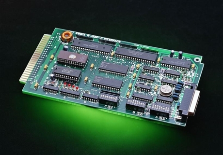
Automotive PCB board process requirements, how to ensure driving safety and stability?

Automotive PCB board technology is an indispensable key link in modern automobile manufacturing. It is directly related to the driving safety and stability of the car. This article will elaborate on the automotive PCB board process requirements from four aspects and discuss how to ensure driving safety and stability.

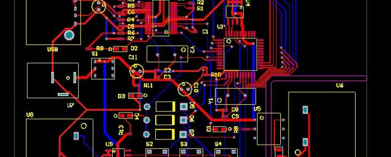
1. Design requirements
Design is the basis of automotive PCB board technology and is related to the stability and reliability of the entire electronic system. The wiring of automobile PCB boards should be reasonable to avoid interference and electromagnetic compatibility issues to ensure the stability of circuit transmission. The impact of environmental factors such as temperature and humidity on the PCB board should also be considered in the design, and appropriate protection measures should be selected, such as moisture-proof, dust-proof, etc., to improve the durability of the PCB board. In addition, the repairability of the PCB board needs to be considered to facilitate later maintenance and upgrades to ensure driving safety.

2. Material selection
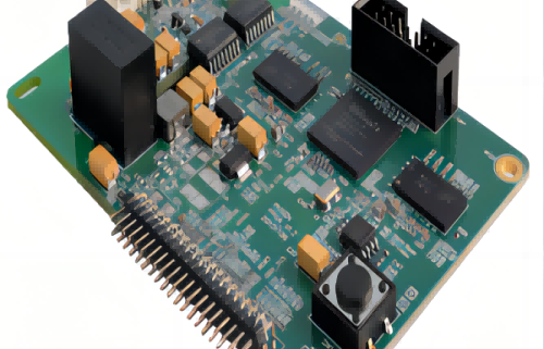
The correct selection of PCB board materials is crucial to ensuring driving safety and stability. Materials with good high-temperature properties should be selected to adapt to the high-temperature requirements of the automotive working environment. The materials should also have lower dielectric loss and better signal transmission performance to improve signal stability. For automotive PCB boards that require fire resistance, materials with better flame retardant properties should be selected to ensure that the fire source can be extinguished in time in the event of an accident. Taking these factors into consideration, selecting appropriate materials can improve the performance and reliability of automotive PCB boards.

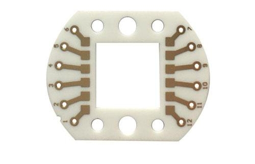
3. Manufacturing process
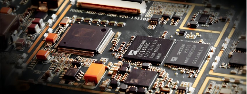
The manufacturing process is a key link in ensuring the quality of automotive PCB boards. A good printed circuit board (PCB) manufacturing process can ensure the accuracy and stability of the circuit and improve the overall quality of the board. A reasonable surface treatment process can improve the connection stability between the PCB board and components, reduce contact resistance, and improve the circuit quality. transmission efficiency. The assembly process of PCB is also very important to ensure welding quality and reliability and prevent circuit failures caused by poor welding. Through good manufacturing technology, the quality and stability of automobile PCB boards can be ensured and driving safety can be improved.

4. Quality control
Automotive PCB board process requirements also require strict quality control measures. Develop and implement strict standards and specifications to ensure that the production of PCB boards meets the specified requirements. Necessary quality inspections and tests are performed during the production process to ensure that every link meets the requirements to reduce the production of defective products. Establish a complete quality traceability system to track and analyze possible quality problems and take corrective measures in a timely manner. Through quality control, PCB board quality problems can be avoided to the greatest extent and the safety and stability of driving can be improved.

Automotive PCB board process requirements play a vital role in ensuring driving safety and stability. Only when all aspects meet the standard requirements can the quality and stability of the automotive PCB board be guaranteed. The automobile manufacturing industry should attach great importance to these requirements in practice, strive to improve the driving safety and stability of automobiles, and provide users with a better driving experience.

What is a car PCB board? What is the difference from a regular circuit board?

Automobile pcb board, that is, printed circuit board for automobiles. As the carrier of on-board electronic equipment, it plays a vital role in the operation of the car. However, what is so special about it that makes it stand out from ordinary circuit boards?

1. Concept and composition of automobile pcb board
Automotive PCB boards are important components used to install electronic components and provide connection paths for various electronic devices and systems in vehicles. It usually consists of a substrate, conductive paths, circuit components, etc. The substrate materials of automotive PCB boards mainly use high-temperature, heat-resistant, moisture-resistant, and corrosion-resistant materials to cope with various challenges in the automotive environment. Conductive paths are usually printed on the substrate. These copper conductive paths are called printed circuits, which connect circuit components and form paths for current flow. Circuit components, such as resistors, capacitors, inductors, diodes, transistors, etc., are key components of automotive circuit boards. They are inseparable from controlling automotive power systems, environmental sensing, navigation and other functions.

2. Application fields of automotive circuit boards
The complexity of modern automobiles far exceeds the mechanical equipment visible to the naked eye of drivers in the past, and automobile PCB boards are used in many fields. For example, the power control system is used to control the entire power system of the car, including the engine, transmission, brakes, etc.; the on-board information system is used to realize navigation, communication, entertainment and other functions; the safety control system involves here including the body stability system, Airbag control, etc.; environment perception systems, such as reversing radar, raindrop detection, etc. Each function requires targeted design and production of automotive PCB boards, which have strict requirements on the performance of automotive PCB boards.

3. Functions and characteristics of automobile pcb boards
The biggest function of the automobile PCB board is undoubtedly to provide connections for electronic components and form a current path for various electronic devices and systems in the automobile. Its performance parameters mainly include high temperature resistance, vibration resistance, humidity resistance, corrosion resistance and other properties. Because of the complexity of the automotive working environment, automotive PCB boards need to cope with a variety of harsh environments such as high temperature, humidity, vibration and impact. Therefore, in terms of material selection and design, there are very high requirements for weather resistance and strength, which are much higher than those of ordinary PCB boards. The circuit board is more powerful.

4. The difference between automobile pcb board and ordinary circuit board
Compared with ordinary circuit boards, automotive PCB boards have significant differences in many properties. The main differences are greater weather resistance and strength. There are higher requirements for the design and production of automobile PCB boards, which need to meet the harsh working environment of automobiles and their complex and changing functional requirements. Automotive PCB boards also have higher vibration resistance and waterproof performance, and pay more attention to environmental protection, because for outdoor equipment such as cars, vibration resistance, waterproofness and environmental protection are particularly important. Automotive PCB boards may be more complex and sophisticated than ordinary circuit boards, because various precise control and adjustment functions in the automotive system need to be implemented by electronic circuits, which requires the circuits to be determined to be more sophisticated and complex.
High temperature resistance, vibration resistance, humidity resistance, corrosion resistance and other properties enable automotive PCB boards to work stably in complex and harsh automotive environments. Compared with ordinary circuit boards, automotive PCB boards are more sophisticated and complex, and meet various functional requirements at the same time, showing their superiority and complexity. Understanding these is of great significance for us to better understand automotive PCB boards and their important role in automotive electronic systems.

PCB wiring analog circuit and digital circuit part

Wiring features:

1. The placement direction of components determines the direction of wiring.

2. The wiring directions of adjacent layers are different. The wiring main body of the surface layer and the welding layer of the two panels is 90?3. The wiring direction of the rectangular circuit board is longitudinal. Horizontal wiring can easily cause congestion or even failure to wire.

4. Try to ensure the wiring space. When this is not possible, use specific components for wiring, and try to avoid connecting holes under the components.

Because when the circuit board fails, it is impossible to visually see the status of the connection holes under the components and whether they are short-circuited with other wiring or component pins.

Analog circuit part and digital circuit part

Including wiring, the analog circuit part and the digital circuit part must be kept above 5mm to ensure that there is no signal interference with each other.

When a symbol is used to represent a ground wire in a circuit diagram, the circuit board designer needs to analyze the circuit diagram and set a certain area. Power cords and ground wires were originally designed. For two-panel and four-layer boards, the wiring composition is completely different. Because the power supply and ground wires are set on the inner layer, attention is mainly focused on them. Just focus on the layout of the signal lines. For beginners, it is recommended to start with the design of four-layer boards. The wiring of power lines and ground wires has a great impact on electricity and noise, so they must be designed carefully.

Take two panels as an example:

○The power cord and ground wire are designed on the same layer, and the effect is very poor

○The ground wire is on the surface and the power wire is on the welding layer. General design

○The ground wire is on the surface, the power wire is on the welding layer, and is wired in copper foil, which has a better anti-clutter effect. Because of the uncontrollability of CAD design, the design takes longer than simple wiring. Pay attention to ensure a small wiring width to ensure that no disconnection or flow obstruction occurs.

To put it simply: the power cord and ground wire are equivalent to the aorta and veins of the human body. You can also simply think of water pipes. The wider the line width, the greater the current flow and faster heat dissipation. The narrower the line width, the greater the resistance under the same voltage, the smaller the current flow that can pass, and the slower the heat dissipation.

Surface welding surface

For power lines and ground wires, large-scale copper foil wiring is used.

Precautions for wiring power lines and ground wires on two-layer circuit boards

Normally, the power wire is routed on the welding surface, the ground wire is routed on the surface, and copper foil is used to wire a wide area, and then some more capacitance is added between the power wire and the ground wire, and there is basically no problem. But if electromagnetic interference is involved, the problem is different. When it exceeds 8MHz, problems of this kind may occur. When it exceeds 25MHz, it will become quite unstable. At this time, it is necessary to surround the important components with ground copper foil, and also design the ground copper foil on the soldering surface.

Crystal oscillator wiring

In order to resist interference, the components should be surrounded by ground copper foil as much as possible. What is not shown in the picture is that ground copper foil can also be laid under the crystal oscillator on the soldering layer, and then the surface and the soldering surface are connected with connection holes. Enhance anti-interference ability.

The use of thermal resistive pads

When power lines and ground wires are routed using large pieces of copper foil, they should be designed using heat-resistant pads as much as possible. This is because if the component pad is directly connected to a large piece of copper foil, the heat will dissipate quickly during welding, and the temperature of the melted solder will not be enough, resulting in poor welding or virtual soldering.

Thermal resistive pad

Power supply for analog circuits

The output part should be close to the power supply. In order to not be affected by the output part, the high-sensitivity input part must be kept at a certain distance from the output part.

Analog circuit diagram Schematic diagram of the separation of digital circuit and analog circuit parts Power input part

DC power supply: When power is provided from the outside, it must first pass through the electrolytic capacitor and then be provided to the internal circuit. The wiring method is usually as follows.

The two-layer panel provides power to the internal circuit not through point A, but through point B. The multi-layer panel also introduces power to the inner layer after passing point B.

Nine rules for high-speed PCB signal routing

In high-speed PCB design, critical high-speed signal lines such as clocks need to be shielded. If there is no shielding or only part of it is shielded, it will cause EMI leakage. It is recommended that shielded wires be drilled and grounded every 1000mil.

Rule 2

High-speed signal routing closed-loop rules

As the density of PCB boards becomes higher and higher, many PCB LAYOUT engineers are more likely to make a mistake during the routing process, that is, high-speed signal networks such as clock signals produce closed-loop results when routing multi-layer PCBs. , such a closed-loop result will produce a loop antenna, increasing the radiation intensity of EMI.

Rule three

Open-loop routing rules for high-speed signals

Rule 2 mentions that the closed loop of high-speed signals will cause EMI radiation, but the open loop will also cause EMI radiation. In high-speed signal networks such as clock signals, once an open loop occurs during multi-layer PCB routing, a linear antenna will be generated, increasing the radiation intensity of EMI.

Rule 4

Characteristic impedance continuity rules of high-speed signals

For high-speed signals, the characteristic impedance must be continuous when switching between layers, otherwise the EMI radiation will be increased. In other words, the width of wiring on the same layer must be continuous, and the impedance of wiring on different layers must be continuous.

Rule five

Wiring direction rules for high-speed PCB design

The wiring between two adjacent layers must follow the principle of vertical wiring, otherwise it will cause crosstalk between lines and increase EMI radiation. In short, adjacent wiring layers follow the horizontal and vertical wiring directions, and vertical wiring can suppress crosstalk between lines.

Rule 6

Topology rules in high-speed PCB design

In high-speed PCB design, the control of the circuit board’s characteristic impedance and the design of the topology under multiple loads directly determine the success or failure of the product. The diagram shows a daisy chain topology, which is generally beneficial when operating at a few Mhz. Star symmetry of the backend is recommended in high-speed PCB designs.

Rule 7

Resonance rules for trace length

Check whether the length of the signal line and the frequency of the signal constitute resonance. That is, when the wiring length is an integer multiple of 1/4 of the signal wavelength, the wiring will resonate, and the resonance will radiate electromagnetic waves and cause interference.

Rule 8

Return path rules

All high-speed signals must have good return paths. Ensure that the return path of high-speed signals such as clocks is as small as possible. Otherwise, radiation will be increased, and the size of the radiation is proportional to the area enclosed by the signal path and the return path.

Rule 9

Device decoupling capacitor placement rules

The placement of the decoupling capacitor is very important. Unreasonable placement will not achieve the decoupling effect at all. The principle is: be close to the pins of the power supply, and the area surrounded by the power supply traces and ground wires of the capacitor is small.

FPC flexible circuit board bending skills help you create tough electronic products!

In the manufacturing process of electronic products, FPC flexible circuit boards play a vital role. Its softness and foldability make the design of electronic products more flexible while also improving the durability of the product. However, bending FPC circuit boards is not a simple task and requires some skills and precautions.

1. Durability of fpc flexible circuit board

FPC flexible circuit boards have outstanding durability, which is mainly reflected in the following aspects.

Excellent flexibility: FPC flexible circuit boards use flexible base materials, so they can work under deformation conditions such as bending, twisting and folding. Compared with rigid circuit boards, fpc flexible circuit boards can adapt to more installation environments, thus improving the durability of the product.

High shock resistance: Due to the flexibility of the FPC flexible circuit board, when subjected to mechanical shock or vibration, compared with the rigid circuit board, the FPC circuit board can better resist and buffer the impact force, thereby reducing the risk of the circuit board risk of damage.

Reliable connectivity: FPC flexible circuit board uses pressure-sensitive adhesive connection method, which has good conductivity and reliability. Even under long-term use and frequent bending, the connection life on the circuit board is guaranteed, thereby increasing the service life of electronic products.

2. Bending skills help create tough electronic products

When using FPC flexible circuit boards for bending processing, the following are some practical tips to help create tough and durable electronic products.

Reasonable design of the bending area: When designing the bending area of the FPC flexible circuit board, the curvature and bending radius of the circuit board need to be fully considered. Reasonable bending area design can reduce stress concentration and reduce the risk of circuit board damage.

Choose the appropriate bending process: For the bending process of FPC flexible circuit boards, there are many methods to choose from, such as manual bending, mechanical bending, etc. According to different product requirements and circuit board characteristics, choosing the appropriate bending process can minimize circuit board damage.

Control the bending force and speed: During the bending process of FPC flexible circuit boards, you need to pay attention to controlling the bending force and speed to avoid excessive force and fast speed causing circuit board rupture. Appropriate force and speed can ensure the integrity and stability of the circuit board.

FPC flexible circuit boards show excellent durability in electronic products, can adapt to various installation environments and resist impact, and extend the service life of the product. At the same time, reasonable bending design and control of the bending process and speed help create tough and durable electronic products. It is believed that FPC flexible circuit boards will play an increasingly important role in the future design and manufacturing of electronic products.

turnkey PCB assembly

What are the uses of printed circuit boards?

Printed Circuit Board (PCB) is a plate-like infrastructure used to connect and support electronic components. In modern electronic equipment, PCB has become the mainstream technology for circuit connection and support of electronic components.

1. Electronic equipment manufacturing
Printed circuit boards are an important part of electronic equipment and are widely used in electronic products, including mobile phones, laptops, desktop computers, digital cameras, televisions and other electronic equipment. Printed circuit boards connect electronic components through current to realize various circuit functions. In the manufacturing process of electronic equipment, printed circuit boards play a key role, and their quality has a great impact on the service life and performance of electronic equipment.
2. Industrial automation
In the field of industrial automation, printed circuit boards are widely used in industrial controllers, sensors and various automation control equipment. Printed circuit boards realize various automated control tasks by combining various circuits to transmit control signals and collect various data.
3. Aerospace
In the aerospace field, printed circuit boards are widely used in high-end equipment such as navigation systems, communication systems, and radar systems. Printed circuit boards must not only meet many technical requirements such as high-speed data transmission and high-precision measurement, but also must meet stringent conditions such as ambient temperature, humidity, and radiation.
4. Medical equipment
Printed circuit boards play an increasingly important role in medical equipment, including medical imaging equipment, life monitoring instruments, etc. As an important part of electronic equipment, printed circuit boards need to meet stringent technical requirements such as safety, accuracy, and stability.
Printed circuit boards are widely used in modern electronic equipment manufacturing, industrial automation, aerospace, medical equipment and other fields. They are an important part of modern high-tech industries. Their technical level is crucial to the development of all walks of life. important role.

PCB board design impedance matching and analysis of the role of zero-ohm resistance.

Impedance matching

Impedance matching refers to a suitable matching method between the signal source or transmission line and the load. There are two ways of impedance matching: serial and parallel according to the access method; impedance matching can be divided into two types: low frequency and high frequency according to the signal source frequency.

High frequency signals generally use serial impedance matching

The resistance of the series resistor is 20~75Ω. The resistance is proportional to the signal frequency and inversely proportional to the PCB trace width. In embedded systems, serial matching resistors are generally required for signals with a frequency greater than 20M and a PCB trace length greater than 5cm, such as clock signals, data and address bus signals in the system, etc. The series matching resistor has two functions:

§Reduce high-frequency noise and edge overshoot. If the edge of a signal is very steep, it contains a large number of high-frequency components, which will radiate interference. In addition, it is also prone to overshoot. The series resistor forms an RC circuit with the distributed capacitance of the signal line and the load input capacitance, which will reduce the steepness of the signal edge.

§Reduce high-frequency reflection and self-excited oscillation. When the frequency of the signal is very high, the wavelength of the signal is very short. When the wavelength is so short that it is comparable to the length of the transmission line, the reflected signal superimposed on the original signal will change the shape of the original signal. If the characteristic impedance of the transmission line is not equal to the load impedance (i.e. does not match), reflection will occur at the load end, causing self-oscillation. The low-frequency signals routed within the PCB board can be connected directly, and there is generally no need to add a series matching resistor.

Parallel impedance matching is also called “terminal impedance matching”

Generally used at the input/output interface, mainly refers to the impedance matching with the transmission cable. For example, when LVDS and RS422/485 use Category 5 twisted pair cables, the input end matching resistance is 100~120Ω; when video signals use coaxial cables, the matching resistance is 75Ω or 50Ω, and when using flat cables, the matching resistance is 300Ω. The resistance of the parallel matching resistor is related to the medium of the transmission cable and has nothing to do with the length. Its main function is to prevent signal reflection and reduce self-oscillation.

It is worth mentioning that impedance matching can improve the EMI performance of the system. In addition, in addition to using series/parallel resistors to solve impedance matching, transformers can also be used for impedance transformation. Typical examples include Ethernet interfaces, CAN buses, etc.

Zero ohm resistor

l It is simply used as a jumper. If a certain section of the line is not used, just do not solder the resistor (it does not affect the appearance).

l When the parameters of the matching circuit are uncertain, use zero ohms instead. During actual debugging, determine the parameters and then replace them with components with specific values.

lWhen you want to measure the operating current of a certain part of the circuit, you can remove the zero-ohm resistor and connect it to an ammeter, which makes it easier to measure the current.

l When wiring, if you really can’t lay it out, you can also add a zero-ohm resistor to act as a jumper.

l In high-frequency signal networks, it acts as an inductor or capacitor (plays an impedance matching role, and zero-ohm resistors also have impedance). When used as an inductor, it is mainly used to solve EMC problems.

lSingle-point grounding, such as single-point connection of analog ground and digital ground to a common ground.

lConfiguration circuit can replace jumpers and DIP switches. Sometimes users will tamper with the settings, which can easily lead to misunderstandings. In order to reduce maintenance costs, zero-ohm resistors should be soldered to the board instead of jumpers.

l For system debugging, for example, divide the system into several modules, and separate the power supply and ground between modules with zero-ohm resistors. When a short circuit is found in the power supply or ground during the debugging stage, removing the zero-ohm resistor can narrow the search range.

The above functions can also be replaced by “magnetic beads”. Although zero-ohm resistors and magnetic beads are somewhat similar in function, they are essentially different. The former has impedance characteristics and the latter has inductive reactance characteristics. Magnetic beads are generally used in power and ground networks to have a filtering effect.

If a worker wants to do his job well, he must first sharpen his tools. A better understanding of impedance matching and zero-ohm resistance will make PCB design and manufacturing easier.

Why is gold plating on PCB boards?

1. PCB board surface treatment:

OSP, HASL leadfree, immersion gold, immersion tin, immersion silver, hard gold plating, full board gold plating, gold finger,ENEPIG,

OSP: lower cost, good solderability, harsh storage conditions, time Short, environmentally friendly technology, good welding, and flat.

HASL leadfree: HASL leadfree boards are generally multi-layer (4-46 layers) high-precision PCB samples. They have been used by many large domestic communications, computers, medical equipment, aerospace companies and research units. Goldfinger (connecting finger) is the connecting component between the memory module and the memory slot. All signals are transmitted through the gold finger.

Gold fingers are composed of many golden conductive contacts. Because the surface is gold-plated and the conductive contacts are arranged like fingers, they are called “gold fingers”.

Gold fingers are actually covered with a layer of gold on a copper-clad board through a special process, because gold is extremely resistant to oxidation and has strong conductivity.

However, due to the high price of gold, currently more memory is replaced by tin plating. Since the 1990s, tin materials have become popular. Currently, almost all “gold fingers” of motherboards, memory and graphics cards are used. Tin material, only some high-performance server/workstation accessory contact points will continue to use gold plating, which is naturally expensive.

2. Why use gold-plated boards?

As ICs become more integrated, IC pins become more dense. The vertical tin spray process is difficult to flatten the thin pads, which makes SMT mounting difficult; in addition, the shelf life of the tin spray board is very short.

The gold-plated pcb just solves these problems:

1. For the surface mount process, especially for 0603 and 0402 ultra-small surface mounts, the flatness of the solder pad is directly related to the quality of the solder paste printing process and has a decisive impact on the subsequent reflow soldering quality. Therefore, the entire board Gold plating is often seen in high-density and ultra-small surface mount processes.

2. In the trial production stage, due to factors such as component procurement, it is often not possible to solder the board as soon as it comes. Instead, we often have to wait several weeks or even months before using it. The shelf life of gold-plated boards is longer than that of lead. Pewter alloy is many times longer, so everyone is happy to use it.

Besides, the cost of gold-plated PCB in the prototyping stage is almost the same as that of lead-tin alloy plate.

But as the wiring becomes denser and denser, the line width and spacing have reached 3-4MIL.

Therefore, the problem of gold wire short circuit has arisen: as the frequency of the signal becomes higher and higher, the signal transmission in multiple coatings due to the skin effect has a more obvious impact on the signal quality.

The skin effect refers to: high-frequency alternating current, the current will tend to flow concentrated on the surface of the wire. According to calculations, skin depth is related to frequency.

In order to solve the above problems of gold-plated boards, PCBs using immersed gold boards mainly have the following characteristics:

1. Because the crystal structures formed by immersion gold and gold plating are different, immersion gold will be golden yellower than gold plating, and customers will be more satisfied.

2. Immersion gold is easier to weld than gold plating and will not cause poor welding or customer complaints.

3. Since the immersion gold board only has nickel and gold on the pad, the signal transmission in the skin effect is in the copper layer and will not affect the signal.

4. Because immersion gold has a denser crystal structure than gold plating, it is less likely to cause oxidation.

5. Since the immersion gold plate only has nickel gold on the pad, it will not produce gold wires and cause short spots.

6. Since the immersion gold plate only has nickel gold on the pad, the solder resist on the circuit is more firmly bonded with the copper layer.

7. The project will not affect the spacing during compensation.

8. Because the crystal structures formed by immersion gold and gold plating are different, the stress of the immersion gold plate is easier to control. For products with bonding, it is more conducive to bonding processing. At the same time, it is precisely because immersed gold is softer than gold plating that gold fingers made of immersed gold pcb are not wear-resistant.

9. The flatness and service life of the immersed gold plate are as good as those of the gold-plated plate.

For the gold plating process, the tin application effect is greatly reduced, while the tin application effect of immersion gold is better; unless the manufacturer requires binding, most manufacturers now will choose the common immersion gold process In this case, the PCB surface treatment is as follows:

Gold plating (electroplating, immersion gold), silver plating, OSP, HASL leadfree.

These types are mainly for boards such as FR-4 or CEM-3. The paper base material and the surface treatment method of coating with rosin; if the problem of poor tin application (poor tin eating) is excluded, solder paste and other patch manufacturers are excluded. Due to production and material technology reasons.

Here we only talk about PCB issues. There are several reasons:

1. When printing PCB, whether there is oil leakage film surface on the PAN position, which can block the effect of tin application; this can be verified by a tin drift test.

2. Whether the PAN position meets the design requirements, that is, whether the pad design can adequately ensure the support of the parts.

3. Whether the pad is contaminated or not, the results can be obtained by using ion contamination test; the above three points are basically the key aspects to be considered by PCB manufacturers.

Regarding the advantages and disadvantages of several methods of surface treatment, each has its own strengths and weaknesses!

In terms of gold plating, it allows the PCB to be stored for a longer time, and is less affected by the external environmental temperature and humidity (compared to other surface treatments), and can generally be stored for about a year; HASL leadfree surface treatment is second, and OSP is third. A lot of attention should be paid to the storage time of the two surface treatments in the ambient temperature and humidity.

Generally speaking, the surface treatment of immersed silver is a little different, the price is also high, and the storage conditions are more stringent, so it needs to be packaged in sulfur-free paper! And the storage time is about three months! In terms of tin application effects, immersion gold, OSP, HASL leadfree, etc. are actually almost the same. Manufacturers mainly consider cost-effectiveness!

How to determine the step of blind and buried vias? How to judge accurately?

PCB blind buried vias are a common type of vias on PCB boards and are also a widely used process in circuit board manufacturing. But what are the step of blind and buried vias? How to judge accurately?

1. What are PCB blind and buried vias?

PCB blind buried vias are a type of via that connects the inner layer traces of the PCB to the surface traces. Blind vias and buried vias are two forms of blind and buried vias in PCB. A blind hole is a kind of via that only connects the inner layer and the surface layer. It needs to reserve a certain depth to facilitate the connection. It can be regarded as a kind of via hole of the inner layer pad. The buried via only connects the inner layer traces inside the PCB. It has nothing to do with the PCB surface traces and is usually used for multi-layer PCBs.

2. Definition of step of PCB blind and buried vias

According to the depth of blind holes or buried holes, blind holes or buried holes can be divided into different orders. First order means that one end of the blind hole can be seen, but the other end cannot be seen. The second level refers to a blind hole where neither end can be seen, but the length can be measured with a tool. At the third level, the length of blind holes and buried holes cannot be seen at all, and the length can only be determined by X-ray measurement.

3. How to accurately determine the step of blind and buried holes in PCB

Accurately judging the order of PCB blind and buried holes requires the use of professional instruments and tools for measurement. Commonly used measurement tools include: high-definition microscopes, solder needles, microscopes, and X-ray inspections. Among them, a high-definition microscope is the most basic tool, which can clearly observe blind holes or buried holes. Solder pins can be inserted into blind holes or buried holes to measure their depth. The microscope is suitable for observing blind and buried holes on complex PCB boards, and X-ray inspection is the most intuitive method, which can clearly observe the internal conditions of blind holes or buried holes.

4. The importance of blind and buried vias in PCB

PCB blind and buried vias are closely related to the electrical performance and reliability of PCB. The connection between the inner layer and the surface layer of the PCB is completed through blind holes. The connection quality of the blind hole well reflects the connection quality between the inner layer and the surface layer. If the order of blind holes is incorrect, it will lead to problems such as poor connections or separation of inner and surface traces, thus affecting the electrical performance and reliability of the PCB. Therefore, it is very important to judge the order of PCB blind and buried vias. Professional measurement tools and detection methods should be reasonably selected to ensure the quality of PCB blind and buried vias.

As an important part of PCB, PCB blind and buried vias directly affect the electrical performance and reliability of PCB. Accurately determining the order of blind and buried vias is very important for the PCB manufacturing process. Reasonable selection of professional measurement tools and detection methods can help us accurately judge PCB blind and buried vias and ensure the reliability and electrical performance of PCB.

What is DBC for ceramic copper-clad pcb?

Direct Bonding Copper is a new type of high-performance heat dissipation material. It is a heat dissipation material that organically combines a copper layer with a ceramic substrate. The copper layer can effectively spread and disperse heat, while the ceramic substrate has good Excellent insulation performance and high temperature stability. DBC has the characteristics of good thermal conductivity, high mechanical strength, good impact resistance, and high temperature resistance. It is widely used in electronic packaging, LED lighting, automotive electronics and other industries.

1. The structure of dbc

The main structure of DBC consists of three parts: metal copper layer, ceramic dielectric layer and metal solder. Among them, the metal copper layer is the main body for electrical conduction and heat dissipation. Its good electrical and thermal conductivity ensures the efficient heat dissipation effect of DBC during use. The metal copper layer adopts the chemical copper plating process, which can form a flat copper layer and have small plastic deformation pressure-sensitive properties, which can effectively maintain the stability of the copper layer throughout the product life cycle. The ceramic dielectric layer plays the role of insulation and mechanical support. Because of its lower thermal conductivity compared to the copper layer, it can ensure that it will not have a great impact on the thermal conductivity of the copper layer. Ceramic substrates mainly use alumina, silicon nitride, ceramic composite materials, etc. These ceramic substrates have the characteristics of good high temperature stability, high mechanical strength, and good corrosion resistance. The metal solder is mainly used to bond the copper layer and the ceramic substrate together, effectively providing the strength of the entire DBC product.

2. Preparation of dbc

The preparation of DBC mainly uses modern electrochemical copperization technology, by forming a layer of active metal substances on the surface of the ceramic substrate, so that the copper layer can be deposited while the copper layer is immersed in the active electrolyte. Commonly used ceramic substrate materials include aluminum oxide and silicon nitride. Among them, DAC-A03 is a ceramic substrate used for high-brightness technology, DAC-A05 is a ceramic substrate used for ordinary technology, and DAC-A07 is a ceramic substrate used for high-precision technology. Compared with silicon nitride, the surface of aluminum oxide is smoother, which can greatly improve the bonding degree and heat dissipation efficiency of the copper layer and the dielectric layer. The combination of ceramic substrate and copper layer mainly uses inkjet printing technology and shielding film technology. Both technologies can realize the preparation of customized DBC products. With the continuous improvement of preparation processes and technological advancement, the performance and stability of DBC products will be further improved.

3. Application of dbc

The applications of dbc mainly cover the fields of electronic packaging, LED lighting and automotive electronics. The field of electronic packaging has always been one of the main application fields of DBC. Because electronic equipment generates a large amount of heat during high-power operation, if the heat cannot be dissipated in a timely and effective manner, the equipment may work unstable or even be damaged. DBC has fast heat dissipation speed and excellent thermal conductivity, and has been widely used in the field of electronic packaging. For example, DBC products can be used in semiconductor power modules, high-power LEDs, power electronic devices, etc. In semiconductor power modules, DBC can be used to package IGBTs, MOSFETs, etc., and the long-term stability and reliability of these devices can be ensured through the DBC heat dissipation structure. With the popularity of LED lamps, dbc is increasingly used in the field of LED lighting. LED lamps also generate a large amount of heat during their working process. This heat can be quickly dissipated to the outside world through DBC, ensuring the high brightness and long life of the LED lamps. Automotive electronic equipment also needs to dissipate heat, and the efficient heat dissipation performance of DBC makes it widely used in the field of automotive electronics.

4. Development prospects of dbc

As a new type of heat dissipation material, DBC has extremely high market value and broad application prospects. With the continuous improvement of the performance of dbc products, it will be widely used in electronics, automobiles, aerospace, medical and energy and other fields. In the electronic field, the functions of electronic products are constantly strengthened and intelligent, which also puts forward higher requirements for heat dissipation performance. This requires dbc, as the main product in the field of electronic product heat dissipation, to continuously advance in technology to meet the needs of the market. . Another example is that in the energy field, DBC also has broad application prospects in solar cells, lithium batteries and fuel cells, because these devices also require an efficient heat dissipation system.

As a new type of heat dissipation material, DBC will be widely used in future development due to its superior heat dissipation performance. With the continuous advancement of technology and continued market demand, the application fields of dbc will become more extensive and the market prospects will become brighter.