Which wiring pattern is better to use when designing PCB?

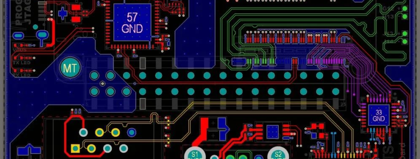
In PCB design, the use of appropriate trace patterns has an important impact on the performance and reliability of the circuit. The following are several common wiring forms. Each has its own advantages. Choosing the appropriate form according to specific design requirements will be more conducive to improving the performance and reliability of the circuit.

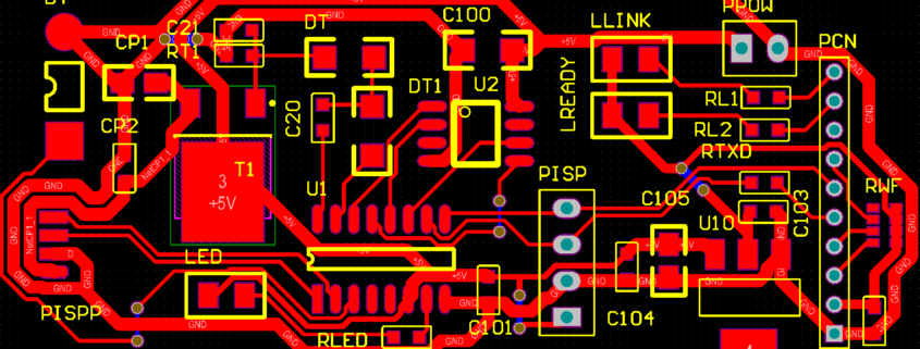
1. Straight-line routing: Straight-line routing is the simplest and most common form of routing. It has the advantage of being direct and fast, which can reduce the delay of signal transmission. In circuit design, there are often some signal lines that must be connected in a straight line, so using straight lines can better meet this requirement.

2. Bend the wiring at a 45-degree angle: When the signal line needs to be introduced into or out of the board, bending the wiring at a 45-degree angle can reduce the reflection and interference of the signal line. Compared to right-angle bends, 45-degree bends can better maintain signal integrity.

3. Arc routing: Arc routing can reduce radiation and crosstalk of signal lines, especially for high-frequency signals. If there are high-frequency signal lines in the design, arc routing can reduce signal loss and distortion.

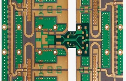
4. Node cross wiring: In design, we often encounter situations where cross signals need to be connected. When conducting node cross wiring, pay attention to the distance between signal lines to prevent signal crosstalk. Interlayer wiring, ground cutting and other methods can be used to reduce signal interference.

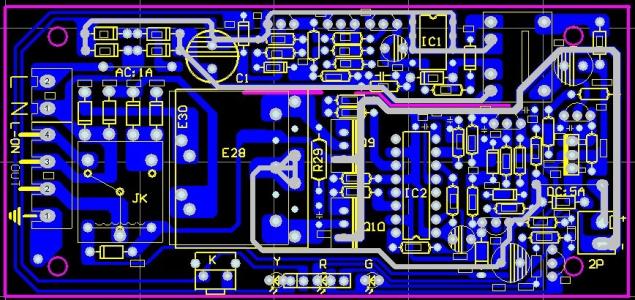
5. Hard-flex wiring: Hard-flex wiring refers to signal transmission through inter-layer connections. It improves design flexibility and reliability. Rigid flexible wiring is widely used in complex high-density circuit design, multi-layer board design, etc.

6. Top/bottom traces: In multilayer board designs, top and bottom traces can be used for shorter signal transmission paths, thereby reducing interlayer vias and delays. At the same time, top/bottom wiring can provide better shielding effect and reduce signal interference.

Although several common wiring forms are listed above, in actual design, multiple factors need to be considered to select the appropriate form. For example, the frequency characteristics of the circuit, noise tolerance, power consumption requirements, and process constraints, etc. When routing, you also need to pay attention to the separation between signals, power supplies, and ground wires, and rationally use ground wire shielding technology.

In short, choosing the appropriate trace pattern is crucial to the performance and reliability of the circuit. Based on the specific design requirements and circuit characteristics, designers should comprehensively consider various factors and select the best wiring form to optimize the circuit design.

How to quickly find GND in PCB?

In the PCB design and production process, finding the ground wire (GND) is a very critical step. GND is a very important reference plane in electronic circuits. It provides a reference level in the circuit and provides a low-noise current path in the circuit. Therefore, finding GND accurately is key to ensuring the circuit works properly. In the following article, we will detail how to quickly find GND in a PCB.

1. GND planning in the PCB design stage:

Before starting to design the PCB, you must first plan the GND. This requires designers to consider the layout of GND during the schematic and layout stages to ensure that the entire circuit is properly laid out on the PCB. When planning GND, there are some principles:

– Try to keep the GND line short and straight. Do not allow GND current to pass through signal lines or other high-frequency lines.

– Minimize the area of the GND loop. A large GND loop will form an antenna and introduce electromagnetic radiation or interference.

– The ground trace opposite the high power source should be wide enough to ensure good current flow throughout the PCB.

– Take care to split the GND into different areas to avoid current interference between different parts.

2. Use a ground plane layer:

The ground plane layer is the layer in the PCB used to form the GND reference plane. It serves to connect individual power pins and other circuit components by creating a continuous copper area between the top and bottom layers of the PCB. During the design process, we can do the following:

– Wrap the entire circuit layout around the ground plane layer, making sure there are no gaps around GND.

– Add GND station holes or GND copper posts near the power pins to strengthen the GND connection.

– Try to use multi-layer boards and use the inner grid layer and ground plane layer to provide a better GND connection.

3. Use GND pin:

On some devices such as power supplies and amplifiers, there will be a dedicated GND pin that is directly connected to the GND reference plane. Properly connecting these pins to the GND plane can help reduce GND voltage drop and noise.

4. Use the remaining electronic connection points:

In some complex circuits, there may be some remaining unused electrical connection points. These connection points are often called electrically sensitive points (ESD). Connecting these connection points to GND can help reduce interference with the circuit.

5. Use the ground test tool:

After the PCB is produced, we can use some ground test tools to confirm the GND connection. These tools can verify GND connectivity by checking that the current flow on the ground wire is smooth and normal.

To sum up, to quickly find the GND in the PCB, we need to carry out reasonable GND planning at the design stage, use the ground plane layer and GND pin to provide a reliable GND connection, and use the remaining electronic connection points and ground test tools to ensure GND for connectivity and reduced interference. Through reasonable design and testing, we can ensure that the GND connection in the PCB is correct and reliable, thereby ensuring the normal operation of the entire circuit.

What should we pay attention to in high-frequency circuit board layout of PCB design?

With the rapid development of electronic technology and the widespread application of wireless communication technology in various fields, high-frequency, high-speed, and high-density have gradually become one of the important development trends of modern electronic products. The high-frequency and high-speed digitization of signal transmission forces PCBs to move towards micropores, buried/blind holes, fine conductors, and uniformly thin dielectric layers.

High frequency circuit board is a special type of circuit board with high electromagnetic frequency. Generally speaking, high frequency can be defined as a frequency above 1GHz. Its various physical properties, accuracy, and technical parameters require very high requirements, and are commonly used in fields such as automotive collision prevention systems, satellite systems, and radio systems. The high-frequency circuit board provided by the utility model is equipped with blocking edges that can block the flow of glue at the upper and lower opening edges of the hollow groove of the core board. In this way, when the core board is bonded with the copper clad board placed on its upper and lower surfaces, the flow of glue will not enter the hollow groove, and the bonding operation can be completed with one press. Compared with the high-frequency circuit board that requires two presses in existing technologies to complete, the high-frequency circuit board in the utility model has a simple structure, Low cost, easy to manufacture.

1. Reasonably select the number of layers

In PCB design, when wiring high-frequency circuit boards, the middle inner plane is used as the power and ground layers to provide shielding, effectively reduce parasitic inductance, shorten signal line length, and reduce cross interference between signals. Generally speaking, the noise of a four layer board is 20dB lower than that of a two layer board.

2. High frequency choke

When wiring high-frequency circuit boards in PCB design, high-frequency choke devices should be connected to common ground wires such as digital ground and analog ground. Generally, high-frequency ferrite magnetic beads with wires threaded through the center hole are used.

3. Signal line

When wiring high-frequency circuit boards in PCB design, signal routing cannot be looped and needs to be arranged in a daisy chain manner.

4. Inter layer wiring direction

In PCB design, when wiring high-frequency circuit boards, the interlayer wiring direction should be vertical, that is, the top layer should be horizontal and the bottom layer should be vertical, which can reduce interference between signals.

5. Number of through-holes

In PCB design, when wiring high-frequency circuit boards, the fewer vias, the better.

6. Copper coating

When wiring high-frequency circuit boards in PCB design, adding copper grounding can reduce interference between signals.

7. Decoupling capacitor

When wiring high-frequency circuit boards in PCB design, decoupling capacitors are connected across the power supply end of the integrated circuit.

8. Wiring length

When wiring high-frequency circuit boards in PCB design, the shorter the wiring length, the better, and the shorter the parallel distance between two wires, the better.

9. Land parcel

In PCB design, wrapping important signal lines can significantly improve the anti-interference ability of signals when wiring high-frequency circuit boards. Of course, it can also package the interference source so that it does not interfere with other signals.

10. Wiring method

In PCB design, when wiring high-frequency circuit boards, the wiring must be rotated at a 45 ° angle to reduce the transmission and mutual coupling of high-frequency signals.

How to design via holes for multi-layer PCB?

Via  is one of the important components of multi-layer PCB, and the cost of drilling usually accounts for 30% to 40% of the PCB board manufacturing cost. Simply put, every hole on the PCB can be called a via. From a functional point of view, vias can be divided into two categories: one is used for electrical connections between layers; the other is used for fixing or positioning devices. From a process perspective, these vias are generally divided into three categories, namely blind vias, buried vias and through vias. Blind holes are located on the top and bottom surfaces of the printed circuit board and have a certain depth. They are used to connect the surface circuits and the inner circuits below. The depth of the holes usually does not exceed a certain ratio (aperture). Buried vias refer to connection holes located on the inner layer of a printed circuit board and do not extend to the surface of the circuit board. The above two types of holes are located in the inner layer of the circuit board. They are completed using the through-hole forming process before lamination. During the via-hole formation process, several inner layers may be overlapped.

The third type is called a through hole, which passes through the entire circuit board and can be used to implement internal interconnections or as mounting positioning holes for components. Because through holes are easier to implement in technology and have lower costs, most printed circuit boards use them instead of the other two via holes. The following via holes are considered as through holes unless otherwise specified.

From a design point of view, a via hole mainly consists of two parts, one is the drill hole in the middle, and the other is the pad area around the drill hole. The size of these two parts determines the size of the via. Obviously, when designing high-speed, high-density PCBs, designers always hope that the via holes should be as small as possible, so that more wiring space can be left on the board. In addition, the smaller the via holes, the smaller their own parasitic capacitance will be. The smaller it is, the more suitable it is for high-speed circuits. However, the reduction in hole size also brings about an increase in cost, and the size of the via hole cannot be reduced indefinitely. It is limited by process technologies such as drilling (drill) and electroplating (plating): the smaller the hole, the harder it is to drill. The longer the hole takes, the easier it is to deviate from the center; and when the depth of the hole exceeds 6 times the drill diameter, there is no guarantee that the hole wall will be evenly plated with copper. For example, if the thickness (through hole depth) of a normal 6-layer PCB board is 50 Mil, then under general conditions, the drilling diameter that the PCB manufacturer can provide can only reach 8 Mil. With the development of laser drilling technology, the size of drilled holes can also become smaller and smaller. Generally, vias with a diameter of less than or equal to 6 Mils are called microvias. Microvias are often used in HDI (High Density Interconnect Structure) design. Microvia technology allows vias to be drilled directly on the pad (Via-in-pad), which greatly improves circuit performance and saves wiring space.

Vias appear as discontinuous impedance breakpoints on the transmission line, which will cause signal reflection. Generally, the equivalent impedance of a via hole is about 12% lower than that of a transmission line. For example, the impedance of a 50-ohm transmission line will be reduced by 6 ohms when passing through the via hole (specifically, it is related to the size of the via hole and the thickness of the board, not reduction). However, the reflection caused by the discontinuous impedance of the via is actually minimal. The reflection coefficient is only: (44-50)/(44+50)=0.06. The problems caused by the via are more concentrated on the parasitic capacitance and inductance. Impact.

2. Parasitic capacitance and inductance of vias

The via itself has parasitic stray capacitance. If it is known that the diameter of the solder mask area of the via on the ground layer is D2, the diameter of the via pad is D1, the thickness of the PCB board is T, and the dielectric constant of the board substrate is ε, then the parasitic capacitance of the via is approximately: C=1.41εTD1/(D2-D1)

The main impact of the parasitic capacitance of the via on the circuit is to prolong the rise time of the signal and reduce the speed of the circuit. For example, for a PCB board with a thickness of 50 Mil, if the diameter of the via pad used is 20 Mil (the drilling diameter is 10 Mils) and the diameter of the solder mask area is 40 Mil, then we can approximately calculate the through hole through the above formula The parasitic capacitance is roughly: C=1.41×4.4×0.050×0.020/(0.040-0.020)=0.31pF. The change in rise time caused by this part of the capacitance is roughly: T10-90=2.2C(Z0/2)=2.2×0 .31x(50/2)=17.05ps

It can be seen from these values that although the effect of slowing down the rise delay caused by the parasitic capacitance of a single via is not very obvious, if vias are used multiple times in the wiring for switching between layers, multiple vias will be used , should be carefully considered when designing. In actual design, parasitic capacitance can be reduced by increasing the distance between vias and copper areas (Anti-pad) or reducing the diameter of the pad.

There are parasitic capacitances and parasitic inductances in vias. In the design of high-speed digital circuits, the harm caused by the parasitic inductance of vias is often greater than the influence of parasitic capacitance. Its parasitic series inductance will weaken the contribution of the bypass capacitor and weaken the filtering effect of the entire power system. We can use the following empirical formula to simply calculate the approximate parasitic inductance of a via: L=5.08h[ln(4h/d)+1] where L refers to the inductance of the via, h is the length of the via, and d is The diameter of the center drill hole. It can be seen from the formula that the diameter of the via hole has a small impact on the inductance, but the length of the via hole affects the inductance. Still using the above example, the inductance of the via can be calculated as: L=5.08×0.050[ln(4×0.050/0.010)+1]=1.015nH. If the rise time of the signal is 1ns, then its equivalent impedance size It is: XL=πL/T10-90=3.19Ω. Such impedance cannot be ignored when high-frequency current flows through it. Special attention should be paid to the fact that the bypass capacitor needs to pass through two vias when connecting the power layer and the ground layer, so the parasitic inductance of the vias will increase exponentially.

3. How to use vias

Through the above analysis of the parasitic characteristics of vias, we can see that in high-speed PCB design, seemingly simple vias often bring great negative effects to the circuit design. In order to reduce the adverse effects caused by the parasitic effects of vias, try to do the following in the design:

1. Consider both cost and signal quality, and choose a reasonably sized via size. If necessary, you can consider using different sizes of vias. For example, for power or ground vias, you can consider using larger sizes to reduce impedance, while for signal traces, you can use smaller vias. Of course, as the via size decreases, the corresponding cost will also increase.

2. From the two formulas discussed above, it can be concluded that using a thinner PCB board is beneficial to reducing the two parasitic parameters of the via.

3. Try not to change layers of signal traces on the PCB board, which means try not to use unnecessary vias.

4. The power and ground pins should be drilled nearby, and the leads between the vias and the pins should be as short as possible. You can consider drilling multiple vias in parallel to reduce the equivalent inductance.

5. Place some grounded vias near the vias of the signal layer to provide a close return path for the signal. You can even put some extra ground vias on the PCB board.

6. For higher-density, high-speed PCB boards, consider using micro vias.

Optimized design techniques for circuit board heat dissipation.

For electronic equipment, a certain amount of heat will be generated during operation, causing the internal temperature of the equipment to rise rapidly. If the heat is not dissipated in time, the equipment will continue to heat up, and the device will fail due to overheating. The reliability of electronic equipment Performance will decrease. Therefore, it is very important to handle the heat dissipation of the circuit board well. The heat dissipation of the circuit board is a very important link.

Optimized design techniques for circuit board heat dissipation

1. Dissipate heat through the PCB board itself

The currently widely used PCB boards are copper-clad/epoxy glass cloth substrates or phenolic resin glass cloth substrates, and there are also a small amount of paper-based copper-clad boards. Although these substrates have excellent electrical properties and processing properties, they have poor heat dissipation. As a heat dissipation path for high-heating components, it is almost impossible to expect the PCB resin itself to conduct heat, but to dissipate heat from the surface of the component to the surrounding air. However, as electronic products have entered the era of component miniaturization, high-density installation, and high-heat assembly, it is not enough to rely solely on the surface of components with very small surface areas to dissipate heat. At the same time, due to the extensive use of surface-mounted components such as QFP and BGA, the heat generated by the components is transferred to the PCB board in large quantities. Therefore, the best way to solve the problem of heat dissipation is to improve the heat dissipation capacity of the PCB itself that is in direct contact with the heating component, through the PCB board Conduct or radiate out.

2. High-heating devices plus radiators and heat conduction plates

When there are a few devices in the PCB that generate a large amount of heat (less than 3), a radiator or heat pipe can be added to the heating device. When the temperature cannot be lowered, a radiator with a fan can be used to enhance heat dissipation. Effect. When there are a large number of heating devices (more than 3), a large heat dissipation cover (board) can be used. It is a special radiator customized according to the position and height of the heating device on the PCB board or placed on a large flat-panel radiator. Cut out the high and low positions of different components. Attach the entire heat dissipation cover to the component surface and make contact with each component to dissipate heat. However, due to the poor consistency of the components during assembly and soldering, the heat dissipation effect is not good. Usually, a soft thermal phase change thermal pad is added to the component surface to improve the heat dissipation effect.

3. For equipment using free convection air cooling, it is best to arrange the integrated circuits (or other devices) vertically or horizontally.

4. Use reasonable wiring design to achieve heat dissipation

Since the resin in the board has poor thermal conductivity, and copper foil lines and holes are good conductors of heat, increasing the remaining rate of copper foil and adding thermal holes are the main means of heat dissipation. To evaluate the heat dissipation capacity of PCB, it is necessary to calculate the equivalent thermal conductivity of the insulating substrate for PCB, which is a composite material composed of various materials with different thermal conductivity.

5. Devices on the same PCB should be arranged according to their heat generation and heat dissipation degree as much as possible. Devices with small heat generation or poor heat resistance (such as small signal transistors, small-scale integrated circuits, electrolytic capacitors, etc.) should be placed in cooling In the uppermost part of the airflow (at the entrance), devices with high calorific value or good heat resistance (such as power transistors, large-scale integrated circuits, etc.) are placed at the most downstream part of the cooling airflow.

6. In the horizontal direction, high-power devices should be placed as close to the edge of the PCB board as possible to shorten the heat transfer path; in the vertical direction, high-power devices should be placed as close to the top of the PCB board as possible to reduce the impact of these devices on the temperature of other devices when they are working. .

7. The heat dissipation of the PCB board in the equipment mainly relies on air flow, so the air flow path must be studied during design and the devices or printed circuit boards should be reasonably configured. When air flows, it always tends to flow in places with low resistance, so when configuring devices on a printed circuit board, avoid leaving a large air space in a certain area. The same issue should also be paid attention to in the configuration of multiple printed circuit boards in the whole machine.

8. Devices that are sensitive to temperature are best placed in the area with the lowest temperature (such as the bottom of the device). Never place it directly above the heating device. It is best to arrange multiple devices staggered on the horizontal plane.

9. Place the devices with the highest power consumption and heat generation near the best heat dissipation locations. Do not place high-heat components in the corners and edges of the PCB unless there is a heat sink arranged nearby. When designing the power resistor, choose a larger device as much as possible, and adjust the PCB board layout to allow enough heat dissipation space.

10. Avoid the concentration of hot spots on the PCB, distribute the power evenly on the PCB as much as possible, and keep the PCB surface temperature performance uniform and consistent. It is often difficult to achieve strict uniform distribution during the design process, but areas with too high power density must be avoided to avoid hot spots that may affect the normal operation of the entire circuit.

What are the basic knowledge of electronic components?

Electronic components are mainly composed of electronic devices and electronic components. Electronic components are components of electronic components and small and medium-sized electrical equipment and instruments. They are often composed of multiple parts and can be used universally in the same industry. The following mainly introduces the basic knowledge of common electronic components.

Basic knowledge of electronic components-resistance

Resistance: The resistance of a conductor to current is called resistance, represented by the symbol R, and the units are ohms, kiloohms, and megohms, represented by Ω, KΩ, and MΩ respectively.

The model naming method of resistors: The model of domestic resistors consists of four parts (not applicable to sensitive resistors) ① Main name ② Material ③ Classification ④ Serial number

The main name, represented by letters, indicates the name of the product. For example, R represents resistance and W represents potentiometer.

Materials, represented by letters, indicate what materials the resistor is made of, T-carbon film, H-synthetic carbon film, S-organic solid, N-inorganic solid, J-metal film, Y-nitride film, C-deposited film , I-glass glaze film, X-wire winding.

Classification is generally represented by numbers, and individual types are represented by letters, indicating what type the product belongs to. 1-normal, 2-normal, 3-ultra high frequency, 4-high resistance, 5-high temperature, 6-precision, 7-precision, 8-high voltage, 9-special, G-high power, T-adjustable.

Serial number, represented by numbers, indicates different varieties of similar products to distinguish the appearance dimensions and performance indicators of the products. For example: R T 1 1 type ordinary carbon film resistor

Classification of resistors: ① wirewound resistors ② thin film resistors: carbon film resistors, synthetic carbon film resistors, metal film resistors, metal oxide film resistors, chemical deposition film resistors, glass glaze film resistors, metal Nitride film resistors ③ Solid resistors ④ Sensitive resistors: varistor, thermistor, photoresistor, force-sensitive resistor, gas-sensitive resistor, humidity-sensitive resistor.

Basic knowledge of electronic components-capacitor

Capacitors are one of the electronic components widely used in electronic equipment. They are widely used in DC blocking, coupling, bypass, filtering, tuning loops, energy conversion, control circuits, etc. Use C to represent the capacitance. The capacitance units include farad (F), microfarad (uF) and picofarad (pF). 1F=10^6uF=10^12pF

Capacitor model naming method The model of domestic capacitors generally consists of four parts (not applicable to pressure-sensitive, variable, and vacuum capacitors). They represent name, material, classification and serial number respectively.

Part 1: Name, represented by letters, capacitor is represented by C.

Part 2: Materials, represented by letters.

Part 3: Classification, generally expressed by numbers, and individually by letters.

Part 4: Serial number, represented by numbers. Use letters to indicate the material of the product: A-tantalum electrolysis, B-polystyrene and other non-polar films, C-high-frequency ceramics, D-aluminum electrolysis, E-other material electrolysis, G-alloy electrolysis, H-composite dielectric, I-glass glaze, J-metallized paper, L-polyester and other polar organic films, N-niobium electrolysis, O-glass film, Q-paint film, T-low frequency ceramics, V-mica paper, Y-mica, Z -paper media

Basic knowledge of electronic components-inductor

The inductor coil is made of wires wound around an insulating tube. The wires are insulated from each other. The insulating tube can be hollow or contain an iron core or magnetic powder core, referred to as an inductor. Expressed by L, the units include Henry (H), milli-Henry (mH), micro-Henry (uH), 1H=10^3mH=10^6uH.

Classification of inductors

Classified by inductance form: fixed inductance, variable inductance. Classified according to the properties of magnetic conductors: air core coils, ferrite coils, iron core coils, and copper core coils. Classified by working nature: antenna coil, oscillating coil, choke coil, notch coil, deflection coil. Classified by winding structure: single-layer coil, multi-layer coil, honeycomb coil.

Main characteristic parameters of inductors

It often works with capacitors to form LC filters, LC oscillators, etc. In addition, people also use the characteristics of inductors to create choke coils, transformers, relays, etc.; the characteristics of inductors are exactly opposite to the characteristics of capacitors. It has the characteristics of preventing alternating current from passing through and allowing direct current to pass through.

There are many inductor coils on the radio, almost all of which are made of air-core coils wound with enameled wire or wound on a skeleton magnetic core or iron core. There are antenna coils (which are made of enameled wire wound on a magnetic rod), intermediate frequency transformers (commonly known as mid-circuit), input and output transformers, etc.

How to solve the heat dissipation problem of PCB circuit board? Master these 10 correct methods.

Controlling heat or heat dissipation and distribution is very important in building and using PCB circuit boards, and failing to manage heat transfer can also ruin your board. For electronic equipment, a certain amount of heat will be generated during operation, causing the internal temperature of the equipment to rise rapidly. If the heat is not dissipated in time, the equipment will continue to heat up, and the device will fail due to overheating. The reliability of electronic equipment Performance will decrease. Therefore, it is very important to handle the heat dissipation of the circuit board well.

1. Heat dissipation through the PCB board itself. The currently widely used PCB boards are copper-clad/epoxy glass cloth base materials or phenolic resin glass cloth base materials, and there are also a small amount of paper-based copper-clad sheets. Although these substrates have excellent electrical properties and processing properties, they have poor heat dissipation. As a heat dissipation path for high-heating components, it is almost impossible to expect the PCB resin itself to conduct heat, but to dissipate heat from the surface of the component to the surrounding air. However, as electronic products have entered the era of component miniaturization, high-density installation, and high-heat assembly, it is not enough to rely solely on the surface of components with very small surface areas to dissipate heat. At the same time, due to the extensive use of surface-mounted components such as QFP and BGA, the heat generated by the components is transferred to the PCB board in large quantities. Therefore, the best way to solve the problem of heat dissipation is to improve the heat dissipation capacity of the PCB itself that is in direct contact with the heating component, through the PCB board Conduct or radiate out.

2. Add radiators and heat conduction plates to high-heating devices. When there are a few devices in the PCB that generate a large amount of heat (less than 3), you can add a radiator or heat pipe to the heating device. When the temperature still cannot drop, A radiator with a fan can be used to enhance the cooling effect. When there are a large number of heating devices (more than 3), a large heat dissipation cover (board) can be used. It is a special radiator customized according to the position and height of the heating device on the PCB board or placed on a large flat-panel radiator. Cut out the high and low positions of different components. Attach the entire heat dissipation cover to the component surface and make contact with each component to dissipate heat. However, due to the poor consistency of the components during assembly and soldering, the heat dissipation effect is not good. Usually, a soft thermal phase change thermal pad is added to the component surface to improve the heat dissipation effect.

3. For equipment that uses free convection air cooling, it is best to arrange the integrated circuits (or other devices) vertically or horizontally.

4. Use reasonable wiring design to achieve heat dissipation. Since the resin in the board has poor thermal conductivity, and copper foil lines and holes are good conductors of heat, increasing the remaining rate of copper foil and adding thermal holes are the main means of heat dissipation. To evaluate the heat dissipation capability of PCB, it is necessary to calculate the equivalent thermal conductivity (nine eq) of the insulating substrate for PCB, which is a composite material composed of various materials with different thermal conductivity.

5. Devices on the same printed board should be arranged according to their heat generation and heat dissipation degree as much as possible. Devices with small heat generation or poor heat resistance (such as small signal transistors, small-scale integrated circuits, electrolytic capacitors, etc.) should be placed In the uppermost part of the cooling airflow (at the entrance), devices with high calorific value or good heat resistance (such as power transistors, large-scale integrated circuits, etc.) are placed at the most downstream part of the cooling airflow.

6. In the horizontal direction, high-power devices should be arranged as close to the edge of the printed board as possible to shorten the heat transfer path; in the vertical direction, high-power devices should be arranged as close to the top of the printed board as possible to reduce the temperature impact of these devices on other devices when they are working. Impact.

7. The heat dissipation of the printed boards in the equipment mainly relies on air flow, so the air flow path must be studied during design and the devices or printed circuit boards should be reasonably configured. When air flows, it always tends to flow in places with low resistance, so when configuring devices on a printed circuit board, avoid leaving a large air space in a certain area. The same issue should also be paid attention to in the configuration of multiple printed circuit boards in the whole machine.

8. Devices that are sensitive to temperature are best placed in the area with the lowest temperature (such as the bottom of the device). Never place it directly above the heating device. It is best to arrange multiple devices staggered on the horizontal plane.

9. Arrange the devices with the highest power consumption and heat generation near the best heat dissipation location. Do not place high-heat components in the corners and edges of the printed board unless a heat sink is arranged nearby. When designing the power resistor, choose a larger device as much as possible, and make sure there is enough space for heat dissipation when adjusting the printed board layout.

10. Avoid the concentration of hot spots on the PCB, distribute the power evenly on the PCB as much as possible, and keep the PCB surface temperature performance uniform and consistent. It is often difficult to achieve strict uniform distribution during the design process, but areas with too high power density must be avoided to avoid hot spots that may affect the normal operation of the entire circuit. If possible, it is necessary to conduct thermal efficiency analysis of printed circuits. For example, the thermal efficiency index analysis software module added to some professional PCB design software can help designers optimize circuit design. The above are some techniques and methods for heat dissipation, which require engineers to continuously accumulate in practice.

Principles for selecting electronic components, how to choose PCB components?

Components are the basic elements that constitute a circuit and are the final result of circuit principle analysis and calculation. In circuit principle analysis, it is necessary to know the structure, characteristics, parameters of each component, its role in the circuit, and its impact on the entire circuit; in circuit parameter calculation, each component parameter is also a factor in circuit calculation. The final result facilitates the reasonable selection of component specifications and models. Correct selection of components is the key to realizing circuit functions, and selection methods and techniques are very important. How to quickly select components in PCB design?

1. Consider the choice of component packaging

Throughout the schematic drawing stage, component packaging and land pattern decisions that need to be made during the layout stage should be considered. Here are some suggestions to consider when selecting components based on their package.

Remember, the package includes the component’s electrical pad connections and mechanical dimensions (X, Y, and Z), which is the shape of the component body and the pins that connect to the PCB. When selecting components, consider any mounting or packaging constraints that may exist on the top and bottom layers of the final PCB. Some components (such as polarized capacitors) may have height headroom restrictions that need to be considered during the component selection process. When you first start designing, you can start by drawing a basic circuit board outline shape, and then place some large or location-critical components (such as connectors) that you plan to use. In this way, a virtual perspective view of the circuit board (without wiring) can be seen intuitively and quickly, and the relative positioning and component height of the circuit board and components are given relatively accurately. This will help ensure that the components fit properly into the outer packaging (plastic, case, frame, etc.) after the PCB is assembled. Call the 3D preview mode from the tools menu to browse the entire board.

The land pattern shows the actual pad or via shape of the soldered device on the PCB. These copper patterns on the PCB also contain some basic shape information. The size of the land pattern needs to be correct to ensure proper soldering and to ensure the correct mechanical and thermal integrity of the connected components. When designing the PCB layout, you need to consider how the board will be manufactured or, if soldered by hand, how the pads will be soldered. Reflow soldering (where flux is melted in a controlled, high-temperature furnace) can handle a wide variety of surface-mount devices (SMDs). Wave soldering is generally used to solder the reverse side of the circuit board to secure through-hole components, but it can also handle some surface-mount components placed on the back of the PCB. Typically when using this technique, the underlying surface mount components must be aligned in a specific orientation, and the pads may need to be modified to accommodate this soldering method.

Component selection can be changed throughout the design process. Determining early in the design process which devices should use plated through holes (PTH) and which should use surface mount technology (SMT) will help with overall PCB planning. Factors to consider include device cost, availability, device area density, power consumption, etc. From a manufacturing perspective, surface-mount devices are generally cheaper than through-hole devices and generally have higher availability. For small and medium-sized prototype projects, it is best to use larger surface-mount devices or through-hole devices, which not only facilitates manual soldering, but also facilitates better connection of pads and signals during error checking and debugging.

If there is no ready-made package in the database, a custom package is usually created in the tool.

2. Use good grounding methods

Make sure the design has adequate bypass capacitors and ground planes. When working with integrated circuits, make sure to use appropriate decoupling capacitors close to the power supply terminals to ground (preferably the ground plane). The appropriate sizing of the capacitor depends on the specific application, capacitor technology, and operating frequency. When bypass capacitors are placed between the power and ground pins and placed close to the correct IC pins, the electromagnetic compatibility and susceptibility of the circuit can be optimized.

3. Assign virtual component packages

Print a bill of materials (BOM) for inspection of virtual components. Virtual components do not have associated packages and will not be passed to the layout stage. Create a bill of materials and view all virtual components in your design. The only entries should be for power and ground signals, as they are considered virtual components and are only handled exclusively in the schematic environment and are not transferred to the layout. Unless used for simulation purposes, components shown in the virtual section should be replaced with components with encapsulation.

4. Make sure you have complete bill of materials data

Check that the bill of materials report contains sufficiently complete data. After the bill of materials report is created, it should be carefully checked to complete any incomplete device, supplier or manufacturer information in all component entries.

5. Sort according to component number

To aid in sorting and viewing the bill of materials, make sure component designations are numbered consecutively.

6. Check for redundant gate circuits

Generally speaking, all redundant gate inputs should have signal connections to avoid floating inputs. Make sure you check any redundant or missing gates and that any unwired inputs are fully connected. In some cases, if the input is left floating, the entire system may not work correctly. Take the dual op amps often used in design. If only one op amp is used in a dual op amp IC component, it is recommended to either use the other op amp, or ground the input end of the unused op amp, and place a suitable unity gain (or other gain ) feedback network to ensure that the entire component can work properly.

In some cases, ICs with floating pins may not function properly within specifications. Typically an IC can operate to meet specifications only if the IC device or other gates in the same device are not operating in saturation and the inputs or outputs are close to or at the component supply rails. Simulation often cannot capture this situation because simulation models generally do not connect multiple parts of the IC together to model the floating connection effect.

Seven factors that affect SMT welding quality.

SMT (Surface Mount Technology) welding is a commonly used welding method in modern electronic manufacturing. However, SMT welding quality is affected by many factors, and these factors often have an important impact on welding quality. Next, we will introduce in detail the seven factors that will affect the quality of SMT welding.

1. Temperature control

In the SMT welding process, temperature control is very important. Too high or too low temperature will cause the welding quality to deteriorate. Generally speaking, the soldering temperature should be adjusted according to the requirements of electronic components and soldering materials. If the temperature is too high, it may cause damage to electronic components or overheat the solder joints, thus affecting the soldering quality. And if the temperature is too low, the welding point may not reach a sufficient melting temperature, causing the welding to be weak.

2. Beating quality

Blurring is an important link in the SMT welding process, which directly affects the welding quality. When applying paste, it is necessary to ensure that the position and size of the solder joints are consistent with the design requirements, as well as the wettability between the paste and the solder joints. If the paste is uneven or excessive, it may result in too many or too few welding points, thus affecting the welding quality.

3. Solder alloy

Selecting the appropriate solder alloy is also one of the key factors affecting SMT welding quality. A common solder alloy is an alloy of tin and lead. However, due to environmental protection requirements, many places have begun to use lead-free solder alloys. The selection of solder alloy should be determined according to the requirements of electronic components and printed circuit boards to ensure soldering quality.

4. Equipment performance

The performance of the equipment used in SMT welding will also directly affect the welding quality. The stability and accuracy of the equipment are crucial to the control of the welding process. The equipment should be able to provide appropriate functions such as temperature control, paste control and welding parameter control to ensure the stability and consistency of welding quality.

5. PCB design

PCB (Printed Circuit Board) design will also have an important impact on SMT welding quality. Reasonable PCB design should consider factors such as the layout of components, the size and shape of the pads, and the distance between the soldering points and components. Improper PCB design may result in component position deviation, pad size mismatch, or improper spacing between soldering points, thereby affecting soldering quality.

6. Maintenance

The maintenance of SMT welding equipment is also one of the key factors to ensure welding quality. Regular inspection and maintenance of equipment to maintain the stability and accuracy of the equipment is very important for the control of welding quality. In addition, timely replacement of worn parts and keeping equipment clean can also effectively improve welding quality.

7. Operator skills

The skill level of the operator will also directly affect the quality of SMT welding. Skilled operating skills can ensure accurate setting of welding parameters and stable control of the welding process. At the same time, operators should have the ability to solve common problems, such as poor welding, solder joint defects, etc., to improve welding quality.

To sum up, SMT welding quality is affected by many factors. Temperature control, paste quality, solder alloy selection, equipment performance, PCB design, equipment maintenance and operator skills are all important factors that affect SMT welding quality. Only by comprehensively considering and reasonably controlling these factors can we ensure that the welding quality during the SMT welding process meets the requirements.

What are the key points of PCB design?

PCB design is a vital part of electronic product development. Here are some PCB design points and key considerations:

1. Layout planning: PCB layout planning is the basis of design. The location of components, wiring routes, power supplies, and ground planes must be considered to ensure signal integrity and optimal performance. Minimize the length of the signal line and reduce the delay of signal transmission.

2. Match impedance: Ensure that the impedance of the signal line matches the signal to be transmitted to reduce reflections and signal integrity issues. Interference can be reduced using differential signaling.

3. Power and ground planes: There should be stable power and ground planes on the PCB to reduce electromagnetic interference (EMI) and provide stability in power distribution. This helps reduce the length of the signal return path.

4. Appropriate layers: Multi-layer PCB can be used to isolate different signals and reduce interference between signal layers. Choose the appropriate layer to meet the needs of your circuit.

5. Thermal management: Consider the heat dissipation needs of components to ensure that heat can be effectively dissipated to avoid component damage caused by overheating.

6. Positioning holes and fixing holes: Add positioning holes and fixing holes to the PCB to install and fix the PCB into a housing or other structure.

7. Symbols and Labels: Add clear symbols and labels to components and connections to facilitate maintenance and troubleshooting.

8. Safety and regulations: Ensure that the PCB design complies with applicable safety standards and regulations, especially for electrical safety and electromagnetic compatibility.

9. EMI suppression: Take necessary measures to reduce electromagnetic interference, such as adding shields, ground planes, filters, etc.

10. Material selection: Select appropriate PCB materials, considering dielectric constant, loss factor and temperature characteristics to meet design needs.

11. Testing and verification: Before actual manufacturing, use simulation tools to verify the performance of the design and conduct prototype testing to ensure that the PCB works properly.

12. Maintainability: Consider the maintainability of PCB to make repair and maintenance work easier.

13. Cost control: Try to reduce PCB manufacturing costs, but do not sacrifice performance and quality.

The importance of PCB design points is to ensure that the circuit board can work properly and have good signal integrity, stability and performance. Therefore, these points need to be carefully considered during the PCB design process.