Strong power is the key to victory! Circuit board thick copper board manufacturer helps you achieve technological breakthroughs!

Circuit board thick copper board is an indispensable key component in electronic equipment. It provides stable electrical connection and good thermal conductivity, providing strong power for the normal operation of the equipment. This article will elaborate on the thick copper board of circuit board from the following four aspects, including material properties, manufacturing process, application fields and future development trends.
1. Material properties
Thick copper boards have excellent electrical conductivity and thermal conductivity. Compared with ordinary circuit boards, thick copper boards have higher current carrying capacity and lower line impedance, and can meet the needs of high-frequency and high-power equipment. In addition, thick copper plates also have good corrosion resistance and mechanical strength, and can operate stably in various harsh environments.
2. Manufacturing process
The manufacturing process of thick copper boards is relatively complex and requires multiple processes. The first is material selection and cutting. Select copper plates with high purity and fine crystallization as raw materials, and use precision cutting equipment to cut them into the required shape. Then comes surface treatment, including chemical cleaning and anti-oxidation treatment to ensure the purity and stability of the circuit board surface. Next comes pattern drawing and copper lamination, using photolithography technology for image transfer, and laminating the copper foil to the substrate through high temperature and high pressure. Finally, there are processes such as drilling, lead-tin plating, printing and testing to complete the manufacturing of the entire circuit board.
3. Application fields
Thick copper boards are widely used in various high-power and high-frequency electronic equipment, including communication equipment, computer equipment, power supply equipment, automotive electronics, etc. In communication equipment, thick copper plates are used to make high-frequency radio frequency modules and antennas; in computer equipment, thick copper plates are used to make high-performance CPU radiators and cooling modules; in power supply equipment, thick copper plates are used to make high-performance Current DC bus and current sampling resistor, etc. Due to its excellent performance, thick copper boards are also widely used in fields such as new energy vehicles and aerospace.


4. Future development trends
With the continuous development and upgrading of electronic equipment, the requirements for circuit boards are becoming higher and higher. In the future, circuit board thick copper boards will continue to develop towards high density, high performance and multi-function. For example, multi-layer stacking technology and new materials are used to achieve a more compact design and higher circuit integration; advanced heat dissipation technology is used to improve heat dissipation efficiency and meet the thermal management needs of new generation equipment; flexible circuit technology is used to achieve Bending and folding expand the application scenarios of circuit boards. To sum up, circuit board thick copper plate is the key to success in electronic equipment and will help technology achieve new breakthroughs in continuous innovation and development.
As a key component in electronic equipment, circuit board thick copper boards have excellent material properties and manufacturing processes. It is widely used in many fields and provides strong power for the normal operation of equipment. With the continuous development and advancement of electronic equipment, thick copper boards will continue to develop in terms of high density, high performance and multi-function, helping to achieve technological breakthroughs. It is believed that circuit board thick copper board manufacturers will continue to provide innovative products and services to meet market demand and promote the development of the electronics industry.

What fields are thick copper PCB used in? Unlock the multi-faceted identity of thick copper PCB!

In recent years, with the rapid development of science and technology, the application scope of PCB (Printed Circuit Board) thick copper plates has gradually expanded, and it has shown an amazing multi-faceted identity in various fields. This article will focus on the PCB thick copper plate and explore its wide range of applications in the electronic field.
1. Power electronics applications
PCB thick copper plate plays a vital role in the field of power electronics. In high-power equipment such as power amplifiers, inverters, and rectifiers, the use of PCB thick copper plates can effectively improve heat dissipation performance and ensure stable operation of the equipment under high loads. Due to its excellent heat dissipation characteristics, PCB thick copper plates are widely used in various industrial power supplies, UPS, transformers and other equipment. In power electronic equipment, PCB thick copper plates can not only provide good heat dissipation effects, but also increase current carrying capacity, reduce resistance and losses, and improve equipment performance and reliability. Therefore, PCB thick copper plate has become one of the indispensable key materials in the power electronics industry.
2. Automotive electronics field
With the rapid development of automotive electronics technology, PCB thick copper plates have also shown strong application potential in the field of automotive electronics. In fields such as electric vehicles, smart driving, and in-vehicle entertainment systems, PCB thick copper plates can provide stable and reliable electrical connections to meet the needs of high-power and high-frequency electronic equipment. In addition, automotive electronic equipment often needs to work in harsh working environments, such as high temperature, high humidity, vibration and other conditions. The high strength, high reliability and stable performance of PCB thick copper plate make it an ideal choice in the automotive electronics industry.


3. Communication equipment applications
In the field of communication equipment, such as base stations, satellite communications, wireless networks and other equipment, PCB thick copper plates also play a key role. Since communication equipment needs to carry high-power, high-frequency signals, the low resistance, high thermal conductivity and stable performance of PCB thick copper plates make them popular in this field. PCB thick copper plates can not only improve the stability and speed of signal transmission in communication equipment, but also reduce the size of the circuit board and improve the integration and performance of the equipment. Therefore, communication equipment manufacturers are increasingly inclined to use PCB thick copper plates to meet the demand for high-power, high-frequency equipment.
4. Aerospace applications
In the aerospace field, the requirements for electronic equipment are more stringent, and the application of PCB thick copper plates is also more prominent. Aerospace equipment needs to have the characteristics of lightweight, high reliability and high temperature resistance, and PCB thick copper plate can meet these needs. PCB thick copper plates can withstand the working environment under harsh conditions such as high temperature, high pressure and strong vibration in aerospace equipment, ensuring the normal operation of electronic equipment. At the same time, PCB thick copper plates can also meet the needs of aerospace equipment for high-power and high-frequency electronic devices, ensuring equipment performance and safety.
PCB thick copper plates are widely used in power electronics, automotive electronics, communication equipment, aerospace and other fields. Its excellent heat dissipation performance, high current carrying capacity and stable performance make it an indispensable and key component in the modern electronics industry. With the continuous advancement of technology and the expansion of application fields, PCB thick copper plates will continue to play an important role in promoting the development and innovation of electronic equipment.

What are the PCB sensors? Sensor PCB board revealed!

1. Overview of sensor pcb board
The sensor PCB board is a circuit board specially used for sensors, mainly used to measure and detect changes in environmental conditions or object characteristics. It realizes signal collection, processing and transmission by combining sensor elements with circuit boards. Among them, common sensor PCBs mainly include temperature sensor PCBs, photoelectric sensor PCBs, pressure sensor PCBs, etc.
2. Temperature sensor pcb
Temperature sensor PCB is mainly used to measure and control the temperature of objects. The sensor elements used are usually thermistors, thermocouples or semiconductor temperature sensors. By tightly integrating sensor components with PCB, real-time monitoring and control of temperature can be achieved, which is widely used in home appliances, automobiles, medical equipment and other fields.
3. Photoelectric sensor PCB
Photoelectric sensor PCB is mainly used to detect the light intensity and position of objects. Common photoelectric sensor PCB types include photoresistor sensor PCB, photodiode sensor PCB, laser sensor PCB, etc. By combining these sensor components with PCB, functions such as measurement of light intensity and position detection of objects can be realized, and are widely used in fields such as automation control and security monitoring.
4. Pressure sensor pcb
Pressure sensor pcb is used to measure pressure changes of gas or liquid. The sensor elements usually use piezoresistive, capacitive or electronic oscillator sensors. By combining these sensor components with PCBs, pressure monitoring and control can be achieved, and are widely used in industrial automation, energy management, environmental monitoring and other fields.
Sensor PCBs play an important role in various fields. By combining with different types of sensor elements, they can achieve accurate measurement and control of physical quantities such as temperature, light intensity, and pressure. With the continuous advancement of technology, sensor PCBs will be more widely used in various industries, bringing more convenience and innovation to our lives and work.

What are the quality inspection requirements for precision circuit board production?

With the development of electronic technology, precision circuit boards have been widely used in various electronic products. To ensure their reliability and quality, we need to conduct strict quality checks. The following will introduce the requirements for precision circuit board quality inspection, including PCB design, material selection, manufacturing process and final testing.

1. PCB design

Good PCB design can minimize wiring problems. In terms of PCB design, we need to pay attention to the following points:

1. Minimize the length and area of the line to avoid line deformation and cross interference.

2. Arrange components reasonably to reduce the impact of component wiring and welding on the circuit.

3. Ensure good grounding in PCB design, and use multi-layer PCB boards to reduce the impact of electromagnetic waves on lines.

2. Material selection

It is crucial to use high-quality materials for circuit boards. In terms of material selection, we need to pay attention to the following points:

1. The selection of PCB board materials should meet the requirements. For example, glass fiber reinforced epoxy resin board (FR4) should comply with IPC standards.

2. PCB board surface treatment must comply with lead-free and RoHS standards.

3. Select good welding materials and metal chemical reactions and coatings to ensure long-term stability.

3. Manufacturing process

The manufacturing requirements for precision circuit boards are very strict. The following are aspects that need attention during the manufacturing process:

1. Strictly control the number of layers, thickness, hole diameter, etc. of the PCB board to ensure process specifications.

2. Strictly control the board processing process to avoid affecting the circuit.

3. Careful proofing and correction to avoid production defects.

4. Final test

After making the circuit board, we need to conduct final testing. During the testing process, we need to pay attention to the following points:

1. All lines must undergo comprehensive testing such as needle point testing, AOI full board inspection, and X-ray inspection to ensure that the circuit board is defect-free.

2. Before assembling electronic products, the circuit board must be subjected to aging testing to eliminate potential problems.

Precision circuit boards are a very important component of modern electronic products. To ensure the quality of these circuit boards, strict control is required in terms of PCB design, material selection, manufacturing process and final testing. Through the precision circuit board quality inspection requirements introduced in this article, we can better ensure the quality and reliability of electronic products.

Why do we need to use a combination of solder paste and red glue processes in SMT patches?

Surface Mount Technology (SMT) is an important technology in modern electronics manufacturing and is mainly used to mount electronic components on printed circuit boards (PCBs).

In SMT, the red glue process and the solder paste process are two commonly used soldering methods. Although their purpose is to fix electronic components on the PCB, these two processes have differences in materials, equipment, operating procedures and product applications. obvious difference.

The use of solder paste and red glue at the same time is also determined based on the soldering characteristics and fixing requirements of different components.

Overview of SMT solder paste and red glue process

1.Red glue process

The SMT red glue process uses the thermal curing properties of red glue. The red glue is filled between the two pads through a printer or dispensing machine, and then solidified and welded through patch and reflow soldering. Finally, when passing through wave soldering, you only need to pass the surface mount surface through the wave peak, and the soldering process can be completed without using a jig.


2.Solder paste process

The SMT solder paste process is a welding process in surface mount technology and is mainly used in the welding of electronic components. SMT solder paste is composed of metal tin powder, flux and adhesive, etc., which can provide good soldering performance and ensure reliable connection between electronic devices and printed circuit boards (PCB).


Application of red glue technology in SMT

1.save costs

A major advantage of using the SMT red glue process is that there is no need to make fixtures during wave soldering, thus reducing the cost of making fixtures. Therefore, some customers who place small batch orders usually require PCBA processing manufacturers to use red glue technology in order to save costs. However, as a relatively backward welding process, PCBA processing plants are usually reluctant to adopt the red glue process. This is because the red glue process needs to meet specific conditions before it can be used, and the welding quality is not as good as the solder paste welding process.

2.Components are larger in size and have wider spacing

When performing wave soldering, the side of the surface mount component is generally chosen to pass through the wave peak, while the side of the plug-in is above. If the size of surface-mounted components is too small and the spacing is too narrow, the solder paste will be connected when soldering over the wave peak, resulting in a short circuit. Therefore, when using the red glue process, it is necessary to ensure that the size of the components is large enough and the spacing should not be too small.


The difference between SMT solder paste and red glue process

1.Process perspective

When using the glue dispensing process, red glue will become the bottleneck of the entire SMT chip processing production line when the number of points is large; when using the glue printing process, AI is required first and then the chip is placed, and the position of the glue printing is The accuracy requirements are very high. In contrast, the solder paste process requires the use of oven racks.

2.quality perspective

Red glue is easy to lose parts for cylindrical or glass-encapsulated parts, and under the influence of storage conditions, red plastic boards are more susceptible to moisture, resulting in parts being dropped. In addition, compared with solder paste, red plastic boards have a higher defect rate after wave soldering. Typical problems include soldering leaks.

3.manufacturing cost

The oven rack in the solder paste process is a larger investment, and the solder on the solder joints is also more expensive than the solder paste. In contrast, glue is a unique expense in the red glue process. When choosing to use the red glue process or the solder paste process, the following principles are generally followed:

● When there are many SMT components and few plug-in components, many SMT patch processing manufacturers usually use the solder paste process, and the plug-in components use post-processing and welding;

● When there are many plug-in components and few SMD components, the red glue process is generally used, and the plug-in components are also post-processed and welded. No matter which process is used, the purpose is to increase production. However, in comparison, the solder paste process has a lower defect rate, but the output is also relatively low.

In the hybrid process of SMT and DIP, in order to avoid the double reflow situation of one side reflowing and wave soldering once, red glue is dotted on the waist of the chip component on the wave soldering surface of the PCB, so that tin can be applied in one step during wave soldering. , eliminating the solder paste printing process.

What is PCB quality system certification?

As we all know, PCB, as the mother of the electronic industry, is very important to electronic products, especially high-layer multi-layer boards, which are mostly the main control boards of some important equipment. Once there is a problem, it can easily cause huge losses. So, when choosing a foundry When processing high-multilayer boards, how should we determine whether a PCB board factory is qualified for production? Usually, you can be sure by looking at the quality system certification of the PCB board factory.

First, ISO 9001 certification—that is, quality management system certification.

ISO 9001 certified

ISO 9001 certification is by far the most mature quality management framework in the world, setting the standard not only for quality management systems but also for overall management systems. It strengthens the management level of the enterprise through the improvement of customer satisfaction and the improvement of employee enthusiasm. It is used to prove that the enterprise has the ability to provide products that meet customer requirements and applicable regulatory requirements. It is a pass for quality evaluation and supervision of enterprises and products.

ISO 9001 certification is a very basic certification in the world. After obtaining it, ordinary electronics factories can generally start production, but PCB board factories cannot, because PCB production can easily produce a lot of waste that pollutes the environment. , therefore, it is also necessary to obtain IS0 14001 certification, which is environmental management system certification.

ISO 14001 certification

ISO 14001 certification is an international standard focusing on environmental management systems. As people’s environmental awareness increases, this standard is recognized by more and more countries and companies. Its core is to require organizations to control factors that affect the environment during the entire process of product design, production, use, scrap and recycling. It is mainly summarized into major aspects: environmental policy, planning, implementation and operation, inspection and corrective measures, and management review.

After obtaining ISO 9001 and IS0 14001 certification, ordinary consumer electronics PCB boards can be produced. So, what if you need to produce automotive electronics PCB boards? At this time, it is necessary to obtain IATF 16949 certification, which is the automotive quality management system certification.

IATF 16949 certification

IATF 16949 certification is a technical specification developed by the international automotive industry organization IATF. It is based on the ISO 9001 quality management system standard and embeds the special requirements of the automotive industry. These manufacturers must have processing and manufacturing activities directly related to the production of automobiles, and through this activity Products can add value. There are strict qualifications for manufacturers that can be certified. Therefore, the implementation of this specification will have a direct impact on automobile companies and their parts manufacturing suppliers.

What if you need to produce medical device PCB boards? It is necessary to obtain ISO 13485 certification, which is the medical device quality management system certification.

ISO 13485 certification

ISO 13485 certification is a globally recognized medical device quality management standard that focuses on quality management systems and is recognized and used as a framework by the medical device industry and regulatory agencies. The ISO 13485 standard provides manufacturers, designers and suppliers to the medical device industry with the necessary framework to demonstrate compliance with regulatory requirements and reduce stakeholder risk. The focus of ISO13485 medical device quality management system is to ensure consistent quality, product safety and sustainable success of your products or services, supporting them with a strong and effective quality management system.

What if you need to produce military PCB boards? Then, you need to obtain GJB 9001 certification, which is the national military standard quality management system certification.

GJB 9001 certification

The GJB 9001 military product quality management system is compiled in accordance with the requirements of the “Military Product Quality Management Regulations” (referred to as the “Regulations”) and on the basis of the ISO 9001 standard, adding special requirements for military products. The release and implementation of military series standards have promoted the rapid development of the construction of military product quality management systems and promoted the improvement of military product quality and reliability levels.

What if we still need to export to Europe and the United States? Then, RoHS and REACH certification are required.

RoHS certification

RoHS certification is a mandatory standard established by EU legislation. Its full name is the “Directive on the Restriction of the Use of Certain Hazardous Components in Electronic and Electrical Equipment.” This standard was officially implemented on July 1, 2006. It is mainly used to standardize the material and process standards of electronic and electrical products, making them more beneficial to human health and environmental protection. The purpose of this standard is to eliminate six substances including lead, mercury, cadmium, hexavalent chromium, polybrominated biphenyls and polybrominated diphenyl ethers in electrical and electronic products, and focuses on stipulating that the cadmium content cannot exceed 0.01%.

REACH certification

REACH certification is the abbreviation of the European Union Regulation “Registration, Evaluation, Authorization and Restriction of Chemicals”. This is a regulatory proposal involving the production, trade, and use safety of chemicals. The regulations aim to protect human health and environmental safety, maintain and improve EU chemical Industrial competitiveness, as well as the innovative ability to develop non-toxic and harmless compounds. Unlike the RoHS Directive, REACH covers a much wider scope and will affect products and manufacturing processes in various industries, from mining to textiles and clothing, light industry, mechanical and electrical industries, etc.

What if the customer also needs the product to be fireproof? Then, manufacturers need to obtain UL certification.

UL certification

The purpose of UL certification is to test the safety of products and help prevent fires and loss of life caused by defective products; through UL certification, companies will directly benefit from UL’s concept of “safety throughout the product life cycle” during the product development stage. We regard product safety as a core element and pursue safer and higher-quality products to gain recognition from domestic and even international markets. Electronic products must be UL certified before entering the international market.

What are the basic rules for PCB board layout and wiring?

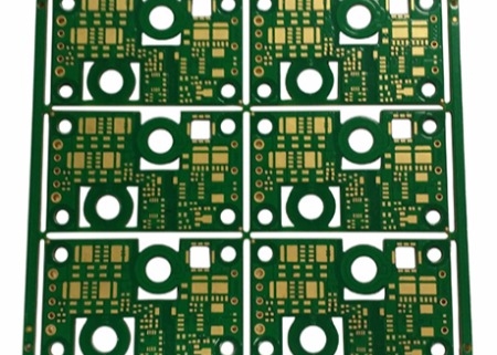
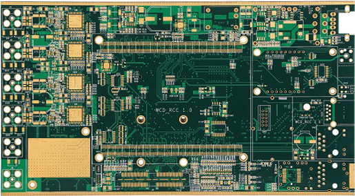
PCB, also known as Printed Circuit Board, can achieve circuit connection and functional implementation between electronic components, and is an important component of power circuit design. Today, this article will introduce the basic rules of PCB board layout and wiring.

1、 Basic rules for component layout

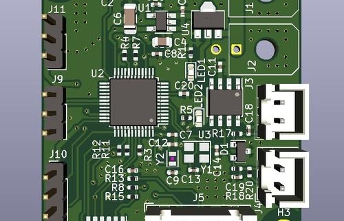
1. Layout according to circuit modules, and related circuits that achieve the same function are called a module. The components in the circuit module should adopt the principle of nearest concentration, and digital circuits and analog circuits should be separated;

2. Elements and components shall not be mounted within 1.27mm around non installation holes such as positioning holes and standard holes, and components shall not be mounted within 3.5mm (for M2.5) and 4mm (for M3) around installation holes such as screws;

3. Avoid placing through holes underneath components such as resistors, inductors (plugins), and electrolytic capacitors installed horizontally to prevent short circuits between the through holes and the component housing after wave soldering;

The distance between the outer side of the component and the edge of the board is 5mm;

5. The distance between the outer side of the solder pad for mounting components and the outer side of adjacent plug-in components is greater than 2mm;

6. Metal shell components and metal parts (shielding boxes, etc.) should not collide with other components, and should not be tightly attached to printed wires or solder pads. The distance between them should be greater than 2mm. The dimension between the outer side of positioning holes, fastener installation holes, elliptical holes, and other square holes in the board and the board edge is greater than 3mm;

7. Heating elements should not be adjacent to wires and thermal sensitive elements; High thermal devices should be evenly distributed;

8. Power sockets should be arranged around the printed circuit board as much as possible, and the wiring terminals of the power sockets and their connected busbars should be arranged on the same side. Special attention should be paid not to arrange power sockets and other welding connectors between the connectors, in order to facilitate the welding of these sockets and connectors, as well as the design and wiring of power cables. The spacing between power sockets and welding connectors should be considered to facilitate the insertion and removal of power plugs;

9. Layout of other components:

All IC components should be aligned on one side, with clear polarity markings for polar components. Polarity markings on the same printed circuit board should not exceed two directions. When two directions appear, the two directions should be perpendicular to each other;

10. The wiring on the board should be appropriately dense. When the difference in density is too large, a mesh of copper foil should be filled, with a mesh size greater than 8mil (or 0.2mm);

11. There should be no through holes on the SMT pad to prevent solder paste loss and component solder failure. Important signal lines are not allowed to pass through the socket pins;

12. Single sided alignment of SMT, consistent character direction, and consistent packaging direction;

13. Devices with polarity should maintain consistency in the direction of polarity markings on the same board as much as possible.

2、 Component wiring rules

1. Within the designated wiring area ≤ 1mm from the edge of the PCB board, as well as within 1mm around the installation holes, wiring is prohibited;

2. The power cord should be as wide as possible and not less than 18 mils; The signal line width should not be less than 12 mils; The CPU input and output lines should not be less than 10mil (or 8mil); The spacing between lines shall not be less than 10mil;

3. Normal through-hole not less than 30mil;

4. Dual in line insertion: 60mil solder pad, 40mil aperture;

1/4W resistor: 51 * 55mil (0805 gauge); When inserting directly, the solder pad is 62mil and the aperture is 42mil;

Unlimited capacitance: 51 * 55mil (0805 surface mount); When inserting directly, the solder pad is 50mil and the aperture is 28mil;

5. Note that the power and ground wires should be as radial as possible, and the signal wires should not have looping.

How to improve anti-interference ability and electromagnetic compatibility?

How to improve anti-interference ability and electromagnetic compatibility when developing electronic products with processors?

1. The following systems need to pay special attention to anti electromagnetic interference:

(1) A system with a microcontroller clock frequency that is particularly high and a bus cycle that is particularly fast.

(2) The system contains high-power, high current drive circuits, such as spark generating relays, high current switches, etc.

(3) A system that includes weak analog signal circuits and high-precision A/D conversion circuits.

2. To increase the system’s ability to resist electromagnetic interference, the following measures are taken:

(1) Choose a microcontroller with low frequency:

Choosing a microcontroller with a low external clock frequency can effectively reduce noise and improve the system’s anti-interference ability. Square waves and sine waves of the same frequency have much more high-frequency components than sine waves. Although the amplitude of the high-frequency component of a square wave is smaller than that of the fundamental wave, the higher the frequency, the more likely it is to be emitted as a noise source. The most influential high-frequency noise generated by microcontrollers is approximately three times the clock frequency.

(2) Reduce distortion in signal transmission

The microcontroller is mainly manufactured using high-speed CMOS technology. The static input current of the signal input terminal is about 1mA, the input capacitance is about 10PF, and the input impedance is quite high. The output terminals of high-speed CMOS circuits have considerable load capacity, that is, a considerable output value. When the output terminal of a gate is led to the input terminal with a relatively high input impedance through a long line, the reflection problem is very serious, which can cause signal distortion and increase system noise. When TPD>Tr, it becomes a transmission line problem that must consider signal reflection, impedance matching, and other issues.

The delay time of the signal on the printed circuit board is related to the characteristic impedance of the leads, that is, to the dielectric constant of the printed circuit board material. It can be roughly assumed that the transmission speed of signals through the leads of printed circuit boards is between 1/3 and 1/2 of the speed of light. The Tr (standard delay time) of commonly used logic telephone components in systems composed of microcontrollers is between 3 and 18ns.

On a printed circuit board, the signal passes through a 7W resistor and a 25cm long lead, with a delay time of approximately 4-20ns on the line. That is to say, the shorter the lead of the signal on the printed circuit, the better, and the longest should not exceed 25cm. And the number of through holes should also be as small as possible, preferably not more than 2.

When the rise time of the signal is faster than the delay time of the signal, it should be processed according to fast electronics. At this point, impedance matching of the transmission line should be considered. For signal transmission between integrated blocks on a printed circuit board, the situation of Td>Trd should be avoided. The larger the printed circuit board, the slower the system speed.

Summarize a rule for printed circuit board design using the following conclusion:

The signal is transmitted on the printed board, and its delay time should not be greater than the nominal delay time of the device used.

(3) Reduce the interactive interference between signal lines:

A step signal with rise time Tr at point A is transmitted to terminal B through lead AB. The delay time of the signal on line AB is Td. At point D, due to the forward transmission of the signal from point A, the reflection of the signal after reaching point B and the delay of line AB, a page pulse signal with a width of Tr will be induced after Td time. At point C, due to the transmission and reflection of the signal on AB, a positive pulse signal with a width twice the delay time of the signal on line AB, that is, 2Td, will be induced. This is the interactive interference between signals. The strength of the interference signal is related to the di/at of the signal at point C and the distance between the lines. When the two signal lines are not very long, what is seen on AB is actually the superposition of two pulses.

Microcontrollers manufactured with CMOS technology have high input impedance, high noise, and high noise tolerance. The superposition of 100 to 200mv noise on digital circuits does not affect its operation. If line AB in the figure is an analog signal, this interference becomes intolerable. For example, if the printed circuit board is a four-layer board, one of which is a large-area ground, or a double-sided board, and the opposite side of the signal line is a large-area ground, the cross-interference between signals will become smaller. The reason is that a large area of ground reduces the characteristic impedance of the signal line, and the reflection of the signal at the D end is greatly reduced. The characteristic impedance is inversely proportional to the square of the dielectric constant of the medium between the signal line and the ground, and directly proportional to the natural logarithm of the thickness of the medium. If the AB line is an analog signal, to avoid the interference of the digital circuit signal line CD to AB, there must be a large area of ground below the AB line, and the distance from the AB line to the CD line should be greater than 2 to 3 times the distance between the AB line and the ground. A partial shielding ground can be used, and ground wires are placed on the left and right sides of the lead on the side with the lead.

(4) Reduce the noise from the power supply

While the power supply provides energy to the system, it also adds noise to the power supply it supplies. The reset line, interrupt line, and other control lines of the microcontroller in the circuit are most susceptible to interference from external noise. Strong interference on the power grid enters the circuit through the power supply. Even in battery-powered systems, the battery itself has high-frequency noise. Analog signals in analog circuits cannot withstand interference from the power supply.

(5) Pay attention to the high-frequency characteristics of printed circuit boards and components

Under high frequency conditions, the distributed inductance and capacitance of the leads, vias, resistors, capacitors, and connectors on the printed circuit board cannot be ignored. The distributed inductance of the capacitor cannot be ignored, and the distributed capacitance of the inductor cannot be ignored. The resistance produces reflection of high-frequency signals, and the distributed capacitance of the lead will work. When the length is greater than 1/20 of the corresponding wavelength of the noise frequency, the antenna effect will occur, and the noise will be emitted outward through the lead.

The vias of the printed circuit board cause a capacitance of approximately 0.6pF.

The packaging material of an integrated circuit itself introduces a 2 to 6 pf capacitance.

A connector on a circuit board has a distributed inductance of 520nH. A dual-in-line 24-pin integrated circuit socket introduces a distributed inductance of 4 to 18nH.

These small distribution parameters are negligible for this line of microcontroller systems at lower frequencies; special attention must be paid to high-speed systems.

(6) Component layout should be reasonably partitioned

The position of components arranged on the printed circuit board must fully consider the issue of anti-electromagnetic interference. One of the principles is that the leads between components should be as short as possible. In terms of layout, the three parts of the analog signal part, the high-speed digital circuit part, and the noise source part (such as relays, high-current switches, etc.) should be reasonably separated to minimize signal coupling between each other.

G Handle the ground wire:

On the printed circuit board, the power and ground wires are the most important. The most important means to overcome electromagnetic interference is grounding.

For double-sided panels, the ground wire layout is particularly particular. By using the single-point grounding method, the power supply and ground are connected to the printed circuit board from both ends of the power supply. There is one contact for the power supply and one contact for the ground. On the printed circuit board, there must be multiple return ground wires, which will all converge on the contact point that returns the power supply, which is the so-called single-point grounding. The so-called separation of analog ground, digital ground, and high-power device ground means that the wiring is separated, and finally they are all gathered at this ground point. When connecting to signals other than the printed circuit board, shielded cables are usually used. For high frequency and digital signals, shielded cables are grounded at both ends. For shielded cables used for low-frequency analog signals, it is best to ground one end.

Circuits that are very sensitive to noise and interference or circuits that are particularly prone to high-frequency noise should be shielded with metal covers.

(7) Make good use of decoupling capacitors.

A good high-frequency decoupling capacitor can remove high-frequency components up to 1GHZ. Ceramic chip capacitors or multilayer ceramic capacitors have better high-frequency characteristics. When designing a printed circuit board, a decoupling capacitor must be added between the power supply and ground of each integrated circuit. The decoupling capacitor has two functions: on the one hand, it is the energy storage capacitor of the integrated circuit, which provides and absorbs the charging and discharging energy at the moment when the integrated circuit opens and closes; on the other hand, it bypasses the high-frequency noise of the device. The typical decoupling capacitor in digital circuits is 0.1uf. The decoupling capacitor has a distributed inductance of 5nH. Its parallel resonance frequency is about 7MHz, which means that it has a good decoupling effect on noise below 10MHz and above 40MHz. Noise has almost no effect.

1uf, 10uf capacitors, the parallel resonance frequency is above 20MHz, and the effect of removing high-frequency noise is better. Where the power enters the printed board and a 1uf or 10uf de-high frequency capacitor is often advantageous, even battery powered systems require this capacitor.

For every 10 or so integrated circuits, a charge and discharge capacitor, or storage and discharge capacitor, is added. The capacitor size can be 10uf. It is best not to use electrolytic capacitors. Electrolytic capacitors are rolled up with two layers of polyurethane film. This rolled structure behaves as an inductor at high frequencies. It is best to use bile capacitors or polycarbonate capacitors.

The selection of the decoupling capacitor value is not strict and can be calculated according to C=1/f; that is, 0.1uf is used for 10MHz. For a system composed of a microcontroller, it can be between 0.1 and 0.01uf.

3. Some experience in reducing noise and electromagnetic interference.

(1) If low-speed chips can be used, high-speed chips are not needed. High-speed chips are used in key places.

(2) A resistor can be connected in series to reduce the upper and lower edge jump rate of the control circuit.

(3) Try to provide some form of damping for relays, etc.

(4) Use the lowest frequency clock that meets system requirements.

(5) The clock generator should be as close as possible to the device using the clock. The quartz crystal oscillator shell must be grounded.

(6) Encircle the clock area with a ground wire and keep the clock wire as short as possible.

(7) Keep the I/O drive circuit as close to the edge of the printed board as possible and let it leave the printed board as soon as possible. The signals entering the printed circuit board must be filtered, and the signals coming from high-noise areas must also be filtered. At the same time, series terminal resistors must be used to reduce signal reflection.

(8) The useless end of MCD should be connected to high, or grounded, or defined as an output end. The end of the integrated circuit that should be connected to power ground should be connected, and should not be left floating.

(9) The input terminal of the unused gate circuit should not be left floating. The positive input terminal of the unused op amp should be connected to the ground, and the negative input terminal should be connected to the output terminal.

(10) Printed boards should use 45-degree fold lines instead of 90-degree fold lines to reduce the external emission and coupling of high-frequency signals.

(11) The printed board is divided according to frequency and current switching characteristics, and the distance between noisy components and non-noise components should be further away.

(12) Use single-point power supply and single-point grounding for single-panel and double-panel panels. The power cord and ground wire should be as thick as possible. If it is affordable, use multi-layer boards to reduce the inductance of the power supply and ground.

(13) Clock, bus, and chip select signals should be kept away from I/O lines and connectors.

(14) Analog voltage input lines and reference voltage terminals should be kept as far away from digital circuit signal lines as possible, especially clocks.

(15) For A/D devices, it is better to unify the digital part and the analog part than to cross.

(16) The clock line perpendicular to the I/O line has less interference than the parallel I/O line, and the clock component pins are far away from the I/O cable.

(17) The component pins should be as short as possible and the decoupling capacitor pins should be as short as possible.

(18) The key lines should be as thick as possible, and protective grounds should be added on both sides. High-speed lines should be short and straight.

(19) Noise-sensitive lines should not be parallel to high-current, high-speed switching lines.

(20) Do not route traces under quartz crystals or devices that are sensitive to noise.

(21) Do not form a current loop around weak signal circuits and low-frequency circuits.

(22) Any signal should not form a loop. If it is unavoidable, make the loop area as small as possible.

(23) One decoupling capacitor per integrated circuit. A small high-frequency bypass capacitor must be added next to each electrolytic capacitor.

(24) Use large-capacity tantalum capacitors or polycrystalline capacitors instead of electrolytic capacitors as circuit charging and discharging energy storage capacitors. When using tubular capacitors, the case must be grounded.

What is the manufacturing process for drone circuit boards?

1、 Material preparation

Before making a drone circuit board, the necessary materials must be prepared first. This includes printed circuit boards (PCBs), electronic components, soldering equipment, etc. Printed circuit boards are the foundation of drone circuits and can be purchased or designed and manufactured by oneself. Electronic components include resistors, capacitors, LEDs, etc., which can be purchased according to one’s own needs. Welding equipment includes welding iron, soldering tin, welding table, etc. It is necessary to choose tools that are suitable for your own use.

2、 Design circuit diagram

After preparing the materials, the next step is to design the circuit diagram. The circuit diagram is the blueprint for the wiring of the drone circuit board, which determines the connection method and working principle of the circuit. Circuit design software such as Eagle and Altium Designer can be used for circuit diagram design, as well as hand drawn circuit diagrams. When designing a circuit diagram, it is necessary to consider factors such as the functional requirements, component layout, and signal transmission of the circuit to ensure its stability and reliability.

3、 Printed circuit board

After completing the circuit diagram design, the next step is to convert the designed circuit diagram into an actual printed circuit board. There are two methods to make printed circuit boards: chemical etching and mechanical milling. The chemical corrosion method requires the use of specific corrosive agents and copper salt solution to print circuit diagrams on copper sheets and remove excess copper layers through corrosion. The mechanical milling rule uses a CNC milling machine to directly mill and engrave the circuit diagram onto the copper plate. Regardless of the method used, it is necessary to pay attention to safe operation to avoid harm to people and the environment.

4、 Welding components

Printed circuit boards will have solder pads, and electronic components need to be connected to the solder pads through soldering. Welding is the process of fixing electronic components and circuit boards together. During the welding process, first apply the solder evenly to the solder pad, then heat the solder with a soldering iron to melt it, insert the electronic components into the solder pad, and use a hot air gun or soldering iron for welding. After welding is completed, it is necessary to check whether the solder joints are even and firm to ensure the reliable connection of the circuit.

Uncover the selection of drone PCB board! How to make wise decisions?

Drones have become a hot topic in modern technology, and more and more people are starting to purchase drones for entertainment, aerial photography, agriculture, security and other fields. However, as one of the core components of drones, the Printed Circuit Board plays a crucial role in determining drone performance and stability. This article will provide a detailed explanation of the selection of drone PCB boards from four aspects, helping readers make wise decisions.

1. Material selection of PCB board

The material selection of PCB boards directly affects the performance and durability of drones. Common PCB board materials include FR-4, metal substrates, ceramic substrates, etc. FR-4 is the most commonly used substrate material with good insulation and heat resistance, suitable for most drone applications. The metal substrate has better heat dissipation ability and is suitable for high-power applications. Ceramic substrates, on the other hand, have excellent insulation and high-frequency performance, making them suitable for applications with high frequency requirements. Choosing suitable PCB board materials for application scenarios can improve the performance and stability of drones.

2. The number of layers and layout of PCB boards

The number of layers and layout of drone PCB boards are also important factors determining their performance. Smaller drones typically use double-layer or four layer PCB boards, while larger or more complex drones require more layers. A reasonable layout can reduce electromagnetic interference and signal crosstalk, and improve the stability and reliability of unmanned aerial vehicle systems. When selecting a PCB board, the appropriate number of layers and layout should be selected based on the needs of the drone and the layout of other electronic components.

3. Quality control of PCB boards

Ensuring the quality of PCB boards is crucial for the performance and reliability of drones. The first step is to choose a reputable PCB board manufacturer and understand their production process and quality control measures. We also conduct professional quality testing, including electrical testing, pad inspection, and circuit tracking. Some high-quality PCB boards also require environmental and reliability testing to ensure they are suitable for working in various complex environments. Only by ensuring the quality of the PCB board is the stability and reliability of the drone system guaranteed.

4. Size and weight of PCB board

For drones, size and weight are also crucial parameters. Excessive size and weight can affect the hovering time and flight stability of drones. Therefore, when selecting a PCB board, the appropriate size and weight should be selected based on the needs of the drone. At the same time, it is also necessary to consider the compactness and durability of the PCB board to ensure the performance and service life of the drone.

How to deal with defective tin on circuit boards?

There are as many as 20 processes in the circuit board design and production process. Poor tin application on the circuit board is really a troublesome problem. Poor tin on the circuit board may cause such problems as line sand holes, line collapse, line dog teeth, open circuits, and small line sand holes. If the copper in the hole is too thin, there will be no copper in the hole; the tin removal is not clean (the number of times of tin withdrawal will affect the plating layer’s tin removal) and other quality problems. Therefore, encountering poor tin application often means that re-soldering is required or even all efforts are wasted. , needs to be remade.


How to deal with defective tin on circuit boards:
Circuit boards will not be properly tinned during SMT production. Generally, poor tinning is related to the cleanliness of the surface of the bare circuit board. If there is no dirt, there will basically be no tinning defects. Secondly, The flux itself is poor when tin is used, temperature, etc.

Improvement and prevention plans for circuit board soldering defects:

1. Regularly test and analyze the ingredients of the potion and add it in time to increase the current density and extend the plating time.

2. Check the anode consumption from time to time and replenish the anode reasonably.

3. Hexagonal cell analysis to adjust the brightener content.

4. Reasonably adjust the distribution of anodes, appropriately reduce the current density, reasonably design the wiring or paneling of the board, and adjust the brightener.

5. Strengthen pre-plating treatment.

6. Reduce the current density and perform regular maintenance or weak electrolysis treatment on the filter system.

7. Strictly control the storage time and environmental conditions during the storage process, and strictly operate the production process.

8. Use solvent to clean the debris. If it is silicone oil, then you need to use a special cleaning solvent for cleaning.

9. Control the temperature during circuit board welding to 55-80°C and ensure sufficient preheating time

10. Use flux correctly.