18-layer of arbitrary interconnect HDI
The PCB industry has experienced years of development, and the technology is gradually maturing and stabilizing. Starting from the newly started single- and double-sided boards, then the multi-layer boards that need to be pressed once, and then to HDI, the integration of PCB products is getting higher and higher!
However, information and communication technology is changing with each passing day. The latest chip manufacturing process has reached 5nm or even 3nm. The faster and faster CPU data processing speed has put higher and higher performance requirements on PCB circuit boards. Those conventional low-level HDI boards can no longer meet the needs of these high-end electronic devices. Therefore, multi-layer, high-level, and even arbitrarily interconnected PCB products have begun to appear in people’s vision.
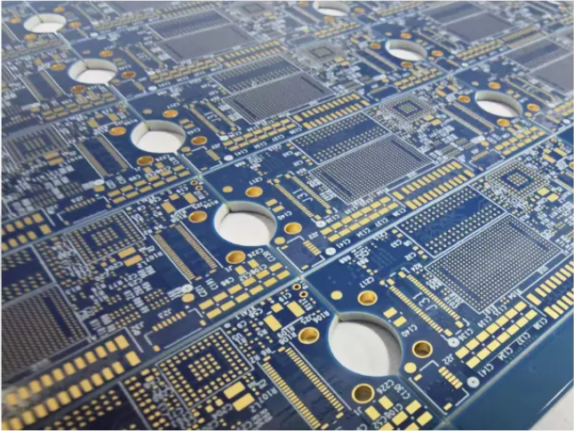
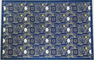
Below is an 18-layer interconnected HDI that we recently produced for a customer. Let’s take a look at its style:
Just looking at the appearance, the dark blue ink is matched with the gold surface of the immersion gold process, and the high-density BGA pads all show its noble temperament! However, his aura does not only come from his appearance. With 18 layers, he contains extremely complex processes inside.
HDI stacking structure: conventional products in the industry are 1-3 order HDI. The more orders, the greater the probability of layer deviation. This product is 18 layers of arbitrary interconnection. Between the layers of the PCB, any layer is connected to each other. There are more than 30 sets of blind holes and buried holes. The design combination is very complex and the processing process is very long.
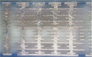
Hole connection method: Through the L9-10 layer core board superimposed 8 times of pressing, superimposed 8 times of laser drilling and electroplating filling, the minimum mechanical aperture is 0.15mm, and the minimum laser aperture is 0.1mm. Let’s take a look at its slice diagram:
Multiple laminations of the core board can easily lead to unlimited expansion and contraction of the core board, resulting in the scrapping of the layer. Therefore, during the lamination process, we are extremely strict in controlling the parameters.
During the production process, we must first consider the circuit pre-release coefficient, which directly affects the production of subsequent boards. Especially in the production of this PCB, since it involves 8 laminations, each lamination will produce a certain expansion and contraction, so it is necessary to adjust the pre-release coefficient to ensure the accuracy and quality of the circuit board. The setting of the pre-release coefficient is one of the key process parameters, which is crucial to ensure the electrical performance and mechanical strength of the PCB!
Interlayer alignment: Due to the large number of layers of HDI boards, ensuring precise alignment between each layer is a huge challenge. Any slight deviation may cause circuit performance degradation or short circuit.
Laser drilling: The laser aperture is 0.1mm. It is difficult for the laser machine to accurately grasp the target position during the expansion and contraction caused by multiple laminations. The laser target and line LDI production parameters of the laser need to be adjusted.
Fine circuit processing: The product circuit is very fine, with a line width and line spacing of 0.06/0.06mm, which requires extremely high processing accuracy. The processing of fine circuits requires the use of high-end processing equipment and sophisticated production technology to ensure the accuracy and stability of the circuit.

